No difficult to get driver ICs, high voltage transistors, inductors, or high voltage transformers: a simple, minimal component count, single digit Nixie clock that fits into glass test-tube case.
Ronald Dekker & Pascal de Graaf
WARNING!
This circuit is directly connected to the mains.
This means that all metal parts in this circuit carry a lethal voltage
with respect to ground. Only operate this clock directly from the mains
if a completely isolated casing is used.
Only build this clock if you have experience with mains operated circuits!
When Pascal de Graaf, a colleague of mine, and I had to make a business to Hamburg some time ago, we had plenty of time to discuss a mutual interest: nixie clocks. Pascal mentioned that he had experienced that one of the biggest hurdles ōto get goingö with nixie tubes is that you need these special and often hard-to-get special components like: high voltage transformers, switch-mode power supplies, special driver ICs or high voltage transistors.
I did not agree with him. According to my opinion it was possible to make a very simple nixie clock without any difficult components. Obviously, I had to prove this statement by demonstrating it. As it happened, I had just finished a single digit clock for my eldest son, and now my youngest son Daan, was begging me if I could also build one for him. The clock described on this page is the result of both events, a simple single digit nixie clock with some interesting features, but without any difficult components.
This clock first of all demonstrates that it is possible to use standard, low-voltage, general puspose, small-signal transistors like the BC550, as nixie drivers. Since I can imagine that it will be a surprise to most people, that a transistor with a BVceo of 50V can be used in a 200V application, I have gone to quite some length to explain it, starting from basic semiconductor theory.
The high voltage supply for the nixie in this clock is directly taken from the mains. This works perfectly, but it has some serious implications with respect to safety. The first section on this page deals with this issue; read it carefully! However, the clock is completely safe as long as a completely isolating case is used, and as long as no metal parts of the circuit can be touched while it is connected to the mains. The circuit for this clock is so small, that an elegant glass test-tube could be used as a case! For safety reasons, the mains on/off switch, in this case a simple cord switch, is used to (besides switch the clock on and off), set the time. How this works is explained later on.
By minimizing the power consumption of the controller circuit, it additionally was possible to feed the low-voltage controller circuit directly from main, without the need for a transformer! How it works is explained in the section
Dropper capacitor power supply.
Figure 1 Impressions from the ambient lighting feature. In reality the effect is not so bright as on the photographs.
The last point concerning this clock that needs introduction is the ambient lighting feature. On the backside of the clock a three color LED is mounted which produces an endless sequence of random colors (Fig. 1). This produces in the evening and at night a nice glow on the wall behind the clock, which really brings the clock to life! I first used this feature in the clock for my son Geert. It was a huge success and you should really try it!
Summarizing, the clock has the following features:
single digit nixie
minimal component design
no hard-to-get driver ICs or high voltage transistors
In a circuit which is directly fed from the mains, the circuit is connected via a direct galvanic
connection to the mains. Before I start with the description of the clock circuit, I have to
explain why directly mains fed circuits are so dangerous, much more dangerous than circuits
that use the same high voltage but derived from a transformer.
Figure 2 Touching a high voltage circuit that is isolated from the mains
is not dangerous as long as no current can flow.
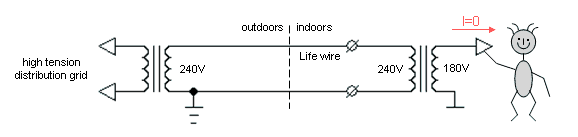
Figure 2 shows a simplified schematic drawing of the final part of the power distribution grid
that delivers the power to your home, connected to an appliance that uses a transformer.
Lets for the sake of this example assume that it is a 240V to 180V transformer used to
feed the NIXIE tubes.
In the last distribution station the high voltage from
the power grid is transformed down to 240V, the mains voltage we have in Europe.
The power is delivered through two wires. One of these wires is called the "life wire" or the
"phase wire". The return wire is called the "null" or "ground" wire. It is important to note
that at the distribution station the ground wire is connected to ground, that is the
ground that you are standing on!
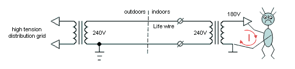
Figure 3 Touching an high voltage circuit at two points closes the loop so that
a current can flow, resulting in a painful if not lethal shock.
When any part of the circuit at the secondary side of the transformer is accidentally touched,
nothing happens since there is no path for the current to flow to ground. The entire circuit is,
although it carries high potential differences, floating with respect to ground. The situation
changes dramatically when accidentally two points in the circuit are touched (Fig. 3).
A large voltage between the points touched will give you a nasty shock or may possibly even kill you!
This is the reason why my father thought me always to keep one hand in my pocket while fiddlingaround with high voltage circuits.
The fact that the secondary side of the transformer is floating with respect to the mains
grid, makes that we can define one of the two terminals as ground and connect it e.g. to the
cassis. In this case we only need to worry about isolating the high voltage derived from the other
transformer terminal.
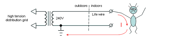
Figure 4 In a circuit that is not isolated from the mains, even a single touch will
result in a flow of current through the ground you are standing !
When no transformer is used, the circuit will always carry a deathly potential with respect
to the real ground (Fig. 4). In this case a single touch to any part of the circuit will
result in the flow of a current straight though your body to ground. This may very easily kill you!
Note that in this case we have no way of knowing which terminal is connected to the live wire
and which terminal is connected to the ground since this will depend on the position of
the mains plug in the wall outlet. Consequently, we have no way of defining one of the terminals as a
local ground. The only solution is to isolate the entire circuit!
It is good for a moment to think of what this really means. It means that you have to treat every
part of the circuit as if it is connected to a lethal voltage with respect to ground,
even if the potential differences in the circuit are small! This is sometimes
a little bit difficult for people to understand. I used to have a neighbor who was in the habit
of decorating his garden with Christmas tree lights. Now, instead of buying decent outdoor type
of lights, he used cheap indoor lights. Being a "they don't fool me" type of man, he argued:
I have 40 lights running on 240V so every light only runs on 240/40=6V, which is not dangerous at all.
Despite my repeated arguments, he was unable to see that although the potential difference across
each lamp might be as small as 6V, the potential difference with respect to ground can be as high as
240V. In other words lethal.
The idea of feeding a circuit directly from the mains is actually very old. The first radios
operated on batteries, one for the filaments and another high voltage battery for the plates
(anodes). The obvious reason was that only few houses were connected to the mains!
Since the current drawn from the anode batteries was usually very small, in the order
of mA's, these batteries only needed replacing every few months or so. Nevertheless, it was cumbersome
and expensive. In the forties almost every body became connected to the mains, so mains
fed power supplies (with transformer) began to replace batteries. Directly after the war everybody
wanted a radio for an affordable price, so radio set makers were forced to cut down production
costs. One of the most expensive parts in a radio was the mains transformer. Set makers came up
with a clever trick to eliminate the transformer.
Instead of making tubes that would run on a
filament voltage of 4 or 6 Volts, they fabricated tubes with a much higher filament voltage so that
when the filaments of all the tubes in a radio were placed in series, they could be directly
connected to the mains. An example of such a radio is the 209U from Philips (
click here to view the schematics ).
Often tube manufacturers would design a set of tubes which together would
make a complete radio while the filaments in series could be connected to the mains. Such a set of
tubes was called a "line up", a term still in use today for e.g. a set of transistors that will
make an RF power amplifier. The same system was adopted for televisions. As explained, a consequence
was that the whole cassis of the set was inevitably connected to the mains, and had to be
completely
isolated. The system was first abandoned for radios. Especially high end radios were provided
with gramophone and tape recorder inputs. These inputs needed a ground connection, so that
isolation from the mains by means of a transformer was unavoidable. For television, the directly
mains fed principle was maintained however throughout the whole tube area. In most modern televisions
the high voltage flyback converter transformer plays the double role of isolating power supply and
high voltage converter.
From the previous section it should be clear that circuits directly fed from the mains
are in principle fine, as long as special precautions are taken for the isolation of the complete
circuit. Special 220V to 220V transformers are ideally suitable for this, but I don't have one.
Instead I use two "low-voltage" transformers back-to-back (Fig. 5a). Transformer T1 is a rather
bulky 10V/4A transformer, T2 is a much smaller 7V/0.7A type. The mismatch
between T1 (10V) and T2 (7v) is explained by considering the resistive losses in T2.
T2 is designed so that it delivers 7V under nominal load conditions. Under nominal conditions
the resistive losses cause a considerable voltage drop in both the primary and secundary
windings of the transformer. The manufacturer of the transformer
added secundary windings to compensate for these losses, so despite the 220V/7V specification,
it really is a 220V/10V transformer (Fig. 5b).
Figure 5 Isolation of a circuit from the mains is ideally done with a special
240/240 (or 110/110) isolation transformer. By placing two normal transformers
back-to-back the same result is archived (Fig. 5a).
Due to voltage drops across the windings (Fig. 5b)
it may me necessary to use transformers with different secondary voltages.
In this section I will try to explain, from basics, what junction breakdown in a diode exactly is, how it compares to the collector-emitter breakdown in a transistor, and why it is that in many applications a transistor can be used for much higher voltages than specified in the datasheet.
The Figures in this section have been taken from a course I have thought at Philips for more than 15 years. They are obviously from the pre-Power Point area. I could never motivate myself to digitize them, sorry!
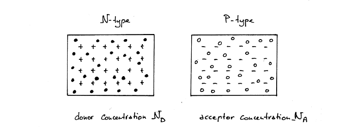
A silicon atom has four electrons in its outer shell. In a silicon crystal, the silicon atoms are all very neatly organized in a lattice, so that every silicon atom shares an electron with its four neighboring atoms. In this way the outer shell is completely filled up with electrons, and there are almost no free electrons for conduction, so pure silicon has a very high resistance.
Figure 6 n-type (left) and p-type (right) silicon.
In the left of Fig. 6, one in every so many silicon atoms has been replaced by another element which has 5 electrons in its outer shell, such as arsenic or phosphorus. This is called ōdopingö of silicon, and since in this case we have an additional negative electron, we call this ōn-type dopingö.
Since this fifth electron can not be shared with any of the neighboring silicon atoms in the lattice, it is free to move through the crystal lattice. When the electron becomes detached from the dopant atom, it leaves behind the positively charged ion fixed in the lattice, in the figure represented by a ō+ö. Note that the silicon atoms have not been drawn in this figure. When an electric field is applied to the crystal, the free electrons will move in a direction opposite to the field, making the silicon conductive.
lternatively, the silicon can be doped ōp-typeö, by replacing the silicon atoms with a ōdopantö like boron, that has only three electons in its outer shell. This open place can be filled by an electron from one of the neighboring silicon atoms, thereby shifting the open place from the boron atom to the silicon atom. When the dopant atom has taken up an electron it becomes negatively charged. This is represented by a ō-ö in the figure. When an electric field is applied to a piece of p-type silicon, electrons will again move in the direction opposite to the electric field, using the empty space on their way. The empty space, more commonly referred to as ōa holeö, however, appears to be moving in the opposite direction, that is in the direction of the field. William Shockley once compared p-type silicon with a car parking with only one empty place left. The only way cars can move on this car parking, is by occupying the empty place. Viewed from high above however, the empty space seems to be moving in a direction opposite to the cars. It has become common practice to consider a hole as the positively charged equivalent of an electron.
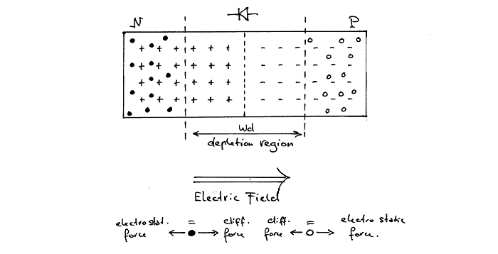
Before continuing, it is important to realize that in a silicon lattice there are only two forces that can make an electron or a hole move. When an electric field is applied over the crystal, the positively charged holes will start to move into the direction of the field, while the negatively charges electrons will move in the opposite direction. This force is called drift of carriers in an electric fiels. The second force is called ōdiffusionö. In a silicon lattice, carriers will tend to move from a location where there is a high concentration to a location with a lower concentration, eventually resulting in a homogeneous distribution. The intricate interplay between drift and diffusion in semiconductors determine their electrical behavior.
Figure 7 The pn-junction with depletion layer at zero bias.
In Fig. 7 an n-type piece of silicon has been brought into contact with a p-type piece of silicon, in such a way that there is no interruption of the silicon lattice between the two parts. Such an arrangement is called a junction. The simplest device consisting of only one junction is called a diode. Initially, there is a high concentration of electrons on the n-type side, while the concentration of holes on the p-type side will be practically zero. This will cause a strong diffusion of electrons from the n-type side to the p-type side. Similarly, a diffusion of holes from the p-type side to the n-type side will take place. At the junction these electrons and holes will ōrecombineö, leaving on the n-type side, fixed in the lattice a positively charged ōdonorö atom, and on the p-type side, a negatively charged ōacceptorö atom. The charged donor and acceptor atoms cause an electric field, which is called the build-in field. Observe, that this electric field exerts a drift force on the electrons and holes that tends to counteract the diffusion force. As more and more electrons and holes recombine, the electric field grows in strength, until a stable situation arises whereby a region is formed that is essentially free of electrons and holes. This region is called the depletion region. At the edges of these regions the diffusion forces are precisely balanced by the drift forces.
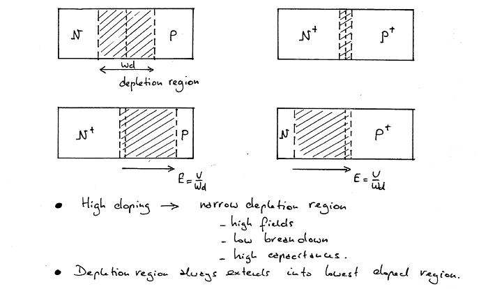
Figure 8 Dependence of depletion layer with on the doping concentration;
the depletion layer always extends into the lowest doped region.
Since during the formation of the depletion region every electron recombines with precisely one hole, the number of charged donors on the n-type side has to equal exactly the number of charged acceptors on the p-type side. This implies that, when the concentration (that is the number per unit of volume) of donors on the n-type side equals the concentration of acceptors on the p-type side, the depletion layer will extend for the same depth into both the n-type side and the p-type side (Fig. 8). When e.g the concentration of donors is higher than the concentration of acceptors (Fig. 8 lower left), a smaller volume of n-type material is needed to provide the same amount of electrons (one electron recombines with one hole). As a rule of thumb we can say that: 1. the higher the silicon is doped, the narrower the depletion region will be and the higher the electric field in the junction, and 2. the depletion layer will extend primarily into the lowest doped region.
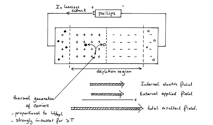
We say that a junction is reverse biased, when an external voltage source, such as a battery, is connected to the junction in such a way the + from the battery is connected to the n-type silicon and the ¢ is connected to the p-type silicon. Observe that in this case the externally applied field has the same direction as the already present internal field, resulting in an increased internal field. To accommodate this increased field, the width of the depletion region will increase (Fig. 9). Ideally, no current will flow in this situation. This is however not exactly true. Every now and then the thermal vibrations of the silicon lattice will free an electron from one of the silicon atoms, resulting in the creation of an electron-hole pair. Due to the electric field, the electron will be quickly removed to the n-type part, while the hole will be removed to the p-type part. Note, that the generation of an electron-hole pair is an extremely rare event, its occurrence determined by statistics. The larger the ōbandgapö of the semiconductor, the rarer the event. Additionally, the higher the temperature, the higher the generation rate. The generation of electron-hole pairs results in a small leackage current in reverse bias.
Figure 9 pn-Juntion under reverse bias,
thermal generation of carriers in the depletion region causes a leakage current.
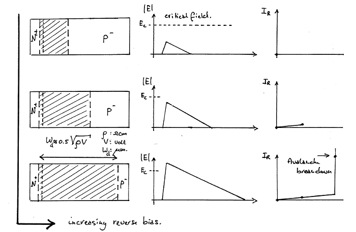
Figure 10 schematically depicts what happens inside a junction when the reverse bias is gradually increased. In this example the n-type side of the junction is more heavily doped (denoted by the n+) than the p-type side (denoted by the p-). As we have seen, the depletion region mainly extends into the lowest doped region. The top row represents the situation when no reverse bias is applied. The middle figure in the top row shows the electric field in the junction. Obviously, the current through the junction is zero in this situation. When a reverse bias is applied (middle row Fig. 10) the depletion region widens, mainly into the lowest doped region. At the same time the maximum electric field in the junction increases. As a result of the thermal generation of carriers, there is a small leakage current flowing through the junction. Although the statistical process of thermal generation of carriers is bias independent, the leakage current nevertheless increases for increasing reverse bias. This is caused by the fact that as the depletion region widens, the volume in which carriers can be generated increasing, resulting in an increase of leakage current.
Figure 10 The depletion region of the pn-Junction under increasing reverse bias.
After the generation of an electron-hole pair, the electron and the hole are accelerated by the electric field. The higher the electric field, the higher the velocity of the carriers. At a certain point the carriers have gained so much energy that they can ionize other silicon atoms on their way, resulting in the creation of an electron-hole pair. These carriers are also accelerated, and can in turn also create electron-hole pairs etc. The result is an exponential increase in current, called ōavalanche breakdownö (Fig. 10 bottom row).
The maximum electric field in a junction is not only determined by the applied reverse bias, it also depends, as we have seen, on the width of the depletion region. A lower doping concentration results in a wider depletion region and thus in a lower field. Diodes with high breakdown voltages therefore have at least one lowly doped region. The price is of course series resistance when the diode is forward biased. Designing a diode (or transistor) is always a matter of carefully balancing tradeoffs.
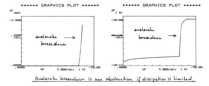
Figure 11 Measured (avalanche) breakdown of a diode plotted on a linear (left) and logarithmic (right) scale.
Figure 11 shows the reverse I-V characteristic of a diode. The left graph shows the I-V curve on a linear scale, while the right graph shows the same I-V on a logarithmic-scale. On a linear scale, the current appears to be practically zero until the diode suddenly breaksdown at approximately 60V; we say it goes into avalanche. On the logarithmic plot we see that leakage current for voltages below breakdown. As predicted, the leakage current slowly increases for increasing reverse bias until it reaches a maximum of ca. 1nA just before breakdown. After breakdown the current is limited by series resistances, and in this measurement the maximum current is limited to 1mA by the measurement equipment.
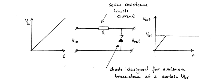
Figure 12 The avalanche breakdown of a diode is non-destructive, and used in zenerdiodes with a working voltage higher than 4.7V to stabilize voltages.
It is important to realize that avalanche breakdown in a diode is by no means a destructive! When the reverse bias is reduced again, the diode
will recover from the breakdown without any damage, provided that the dissipation in the diode is limited to such a value so that the diode is not damaged due to overheating. In fact avalanche breakdown determines the working voltage of all zener diodes for voltages of 4.7V and higher.
Figure 12 depicts how a zener diode can be used a voltage reference. When the input voltage of the circuit is increased, the zener diode, which is nothing else than a normal diode engineered to yield a breakdown at a very specific value, breakdown. The resistor is added to limit the current and thus the dissipation (I*Vbr). Since the I-V curve of te avalanche breakdown is so very steep (Fig. 11 right), the output voltage will be constant over a large range of the current.
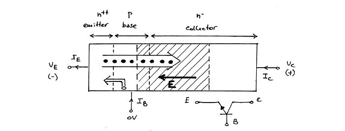
Figure 13 briefly explains the working of a bipolar transistor. It consists of two junctions: the emitter-base junction and the collector-base junction. In an npn transistor, the emitter is n-type doped, the base p-type, and the collector n-type again. Note that there is a difference in doping concentration. The emitter is more heavily doped than the base, while the base in turn is more heavily doped than the collector. The emitter-base junction is normally forward biased. This results in a flow of holes from the base into the emitter (the base current), and a flow of electrons from the emitter into the base. On the other side of the base, which usually is very thin, we have the collector-base junction. The collector-base junction is normally reverse biased. The electrons that have been injected by the emitter into the base never reach the base contact, because when they come into the vicinity of the collector-base junction, they are swept away to the collector by the strong field in the reverse biased collector-base junction (the collector current). The electron (collector) current is much higher than the hole (base) current, because the emitter is more heavily doped than the base. Although they differ in magnitude, the ratio between the electron and hole current (collector and base current) is constant, independent of emitter-base bias, because both currents are governed by the same equations. This ratio is called the current gain of the transistor.
Figure 13 Current amplification in an npn transistor under normal operating conditions.
When a transistor is used as a nixie driver, it is used in two different modes: on or off. When the transistor is switched on, the collector voltage is very low and of no consideration. However, when the transistor is off, the collector ōseesö the high voltage supply of the nixies. It is in this mode that a breakdown can occur. We will now discuss the behavior of the transistor when it is switched off.
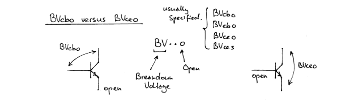
Figure 14 Definition of the different breakdown voltages in a transistor.
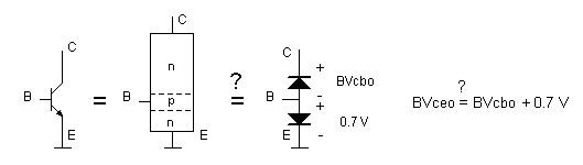
In a diode we only had to deal with one breakdown voltage. In a transistor we have at least two junctions, so we can have a reverse breakdown of the emitter-base junction and of the collector-base junction. These breakdown voltages are usually denoted by something like: BVebo. ōBVö Obviously stands for Breakdown Voltage, ōebö specifies emitter-base junction, while the ōoö means that the breakdown voltage has been measured with the third terminal, the collector, open (not connected). Similarly BVcbo gives the the breakdown voltage of the collector-base junction with open emitter.
The two junctions in the transistor introduce a third possibility for a breakdown, namely between collector and emitter. It is this breakdown that, when the transistor is used as a switch or amplifier, determines the maximum supply voltage. So what determines the collector-emitter breakdown or BVceo?
Figure 15 This over-simplified model does not predict the correct BVceo value.
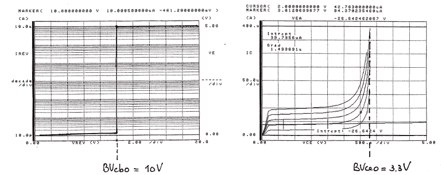
We can first try to make an ōeducated guessö, by representing the transistor in its off state by two diodes placed back-to-back in series (Fig. 15), the lower diode being the emitter-base junction, and the other diode the collector-base junction. LetÆs assume for the moment the validity of this equivalent circuit. In this case the collector-base junction is reverse biased, while the emitter-base junction is forward biased. We would expect that the breakdown voltage between the collector and the emitter would be equal to the collector-base breakdown voltage plus the forward emitter-base junction voltage drop (ca. 0.8 V). In other words we expect the BVceo to be slightly higher than the BVcbo. Rather unexpectedly the opposite is true. Fig. 16 shows a measurement of both the BVcbo (left graph) as well as the BVceo (right graph) of a high frequency transistor. While the BVceo is about 10V the BVceo is only 3.3V! Obviously the simple model that was assumed in Fig. 15 is not valid.
Figure 16 BVcbo (left) and BVceo (right) of a high frequency transistor.
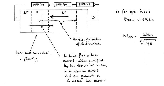
In reality a transistor is not just a series connection of two diodes back-to-back, rather the junctions have been carefully arranged so as to yield a current amplifying device! Fig. 17 shows a bipolar transistor under reverse bias with open base. Since the collector-base junction is reverse biased, most of the applied voltage between the collector and emitter will drop over the collector-base junction. In this junction electron-holes paires will be generated as discussed before. The electric field in the junction will accelerate the electrons towards the collector contact where they will contribute to the leakage current. The holes however, will be accelerated towards the base. On arrival in the base, the holes have nowhere to go, since the BVceo is measured with open base. As a result the base will be charged, and the transistor will be switched on resulting in a large emitter current. A more exact description is: ōthe holes generated in the collector-base junction are, after arrival in the base, injected in the emitter, resulting in an electron current of hFE times the hole current.ö In other words, the transistor is amplifying its own leakage current. What it boils down to is that the BVceo is reduced with respect to the BVcbo by a factor depending on the DC current amplification (Fig. 17).
It is the BVceo that is usually specified in datasheets as being the maximum allowed working voltage.
Figure 17 Under reverse bias, and with open base, the transistor amplifies the thermally generated leakage current,
resulting in a decreased breakdown voltage.
However, the transistor is very rarely being used with an open base! In most cases, and certainly in all cases where the transistor is used as a nixie driver, the base is driven from a low impedance source such a controller or decoder output. In these cases, the hole current just leaks away through the base contact into the device connected to the base. As a result, the emitter-collector breakdown voltage will be almost equal the much higher collector-base breakdown!
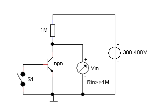
Similar to avalanche breakdown in a diode, avalanche breakdown in a transistor is also non-destructive, provided that the dissipation in the dissipation transistor does not exceed the maximum specifications. This fact can be used to measure the BVceo in a very simple way. In Fig. 18 the npn transistor to be tested is forced into avalanche breakdown by the high-voltage power supply. Assuming a breakdown voltage in the order of 100V, the resistor limits the avalanche current to something in the order of 0.1-0.3mA. This limits the dissipation to a safe value of less than 50mW. The BVceo is now simply the voltage drop across the transistor. In order not to influence the measurement, a multi-meter with a resistivity much higher than 1M has to be used for this method.
Figure 18 Test circuit for the measurement of the BVceo and BVcbo of a transistor.
By closing the switch the BVcbo is measured. It is this value that will determine the maximum voltage drop over the transistor in nixie driver circuits and in fact in most other circuits as well. For example, the BC550 transistor that is used in this clock is specified in the datasheet for a BVceo of 45V. This includes a generous margin for process tolerances, since the real BVceo was measured to be 60V. The BVcbo appeared to be 120V, which will make it a very nice nixie driver.
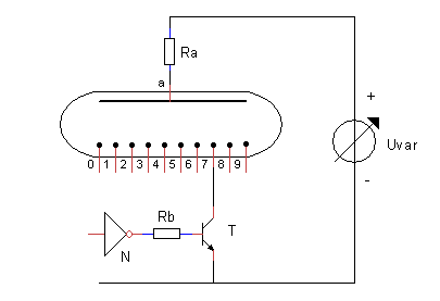
Driving Nixies with ōlow voltageö transistors
Figure 19 shows the basic nixie driver circuit. The base of the transistor is driven by a low output impedance buffer or micro-controller output. In this case, as we have seen, the breakdown voltage between the collector and emmiter will be equal to the collector-base breakdown, which for the BC550 is approximately 120V. When Uvar is increased, the voltage will be devided over the transistor and the nixie tube, since both will have a very high impedance in their off-state. The way Uvar is divided over both components is difficult to predict, but one thing is clear: in order for the nixie to ignite, the total supply voltage has to be at least the nixie ignition voltage (ca. 150V) plus the collector-base breakdown voltage BVceo, of the transistor (ca. 120V). So for supply voltages below 150+120=270V the transistor will not breakdown, but behave as a perfect nixie driver.
Figure 19 Basic nixie driver circuit
The circuit of Fig. 19 can be used to test this concept. Feel free to increase Uvar to beyond the point where breakdown occurs, in this case ca. 270V. Just as in the case of avalanche breakdown in a diode, also avalanche breakdown in a transistor is non-destructive. Note however, that since the voltage over the transistor is high (= BVcbo = 120V) already a small current of 1mA will cause a dissipation of 120mW, which is about the specified maximum for most ōsmall-signalö transistors.
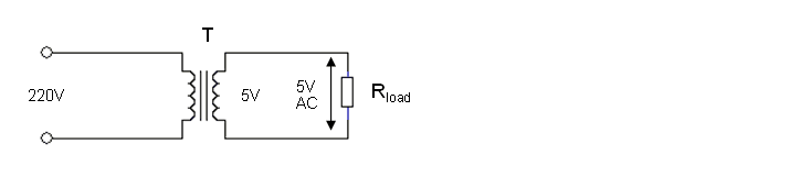
In most low voltage power supplies a transformer is used to perform the tasks of: 1. voltage transformation and 2. isolation of the low voltage circuit from the mains (Fig. 20). As explained in the section on safety, this isolation is needed so that the circuit can be safely touched. Since for this clock I already decided to derive the high voltage supply for the nixies directly from the mains, and as a consequence to use a fully isolated case, it became possible, even logical, to see if also the low voltage supply could be directly derived from the mains.
Figure 20 Low-voltage power supply using a transformer
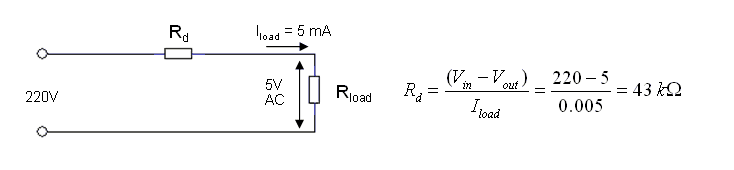
Instead of using a bulky transformer that would certainly not fit into the test tube I had in mind for the case, a so called dropper capacitor is used. This section explains how it works and what its limitations are.
Figure 21 Low-voltage power supply using a dropper resistor
The simplest way to reduce the 220V mains voltage to something like the 5V needed to power the micro-controller and some peripheral logic, is to simply drop the voltage surplus over a suitable series resistor (Fig. 21). The biggest drawback of this solution is obviously dissipation. Even if we assume that the total circuit would not consume more than 5mA, this will result in a dissipation of (220-5)*0.005=1.075W. Considering the fact that the circuit itself dissipates only 0.005*5=0.025W, the efficiency of this power supply would be something like 2%, which is, apart from the problems associated with the generated heat, an absolute waste of power.
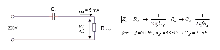
Figure 22 Low-voltage power supply using a dropper capacitor
A much more sensible solution is to replace the resistor by a suitable capacitor. Looking at Fig. 22, we observe that the circuit basically has become a low-pass filter, which is dimensioned in such a way that only just enough current passes to cause a voltage drop of 5V over the load, while the remaining 215V drops over the ōdroppingö capacitor. The beauty of this solution is that since the phase of the current through a capacitor is shifted 90 degrees with respect to the voltage across it, the dissipation in the capacitor will be zero.
That is for an ideal capacitor, in reality every capacitor will have some series resistance, resulting in a very small dissipation. This however is nothing compared to the dissipation in a dropper resistor.
The value of the capacitor is chosen such that its impedance given by 1/(2*pi*f*C) equals the resistance of the dropper resistor that otherwise would have been needed (Fig. 22). The idea is already very old. A dropper capacitor was a favored trick of my father to make a simple low-cost power supply, for instance for trickle chargers. He used to keep a scrap-book with clippings of schematics and pictures of circuits he found interesting or useful and the picture on the left, taken from ōRadio Bulletinö was certainly one of them.
The main limitation of this idea, apart from its lack of isolation from the mains, is that the use of a dropper capacitor only makes sense for low-current applications. The larger the current required, the higher the capacitance value needed. Capacitors will values higher than 1.0uF, rated for voltages of 400-600V are expensive, bulky and sometimes difficult to get. So for currents higher than 20-30mA, a small transformer will already be a more economical (and much safer) solution.
Figure 23 Adding a zener diode to the dropper capacitor results in a pulsating DC voltage.
By adding a simple zenerdiode to the circuit, the output voltage is stabilized while at the same time it is rectified to a (pulsating) DC voltage. In Fig. 23 we see that during the positive period of the voltage, the zenerdiode limits the voltage to a value corresponding to its breakdown voltage. During the negative period, the zenerdiode will be forward biased, so that the voltage drop will be something like 0.6V, resulting in a pulsating DC voltage. The zenerdiode needs a few mA to operate correctly, so that the value of the dropper capacitor has to be a little bit larger than needed for the load alone.
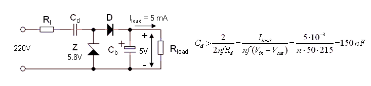
Figure 24 Final low-voltage power supply using a dropper capacitor.
The purpose of resistor Rl is to limit the current through the capacitor and the zenerdiode when the circuit is switched on. Assume for the moment that Cd is completely discharged, and that the mains voltage is applied at one of the maxima during the 50Hz cycle. Without Rl this would result in a very large transient current, only limited of by the parasitic resistances of the capacitor and the zenerdiode. This current could easily kill the zenerdiode, and probably the complete circuit behind it.
The value of Rl is selected such that at the maximum peak mains voltage of sqrt(2)*220= 310V, it will limit the peak current through the diode to the maximum allowed value, usually around 1A. In most cases a value of 470-1k is sufficient.
Note, that the value of Cd as given by the equation in Fig. 24 is twice the value as given by the equation in Fig. 22. The reason for this is that only the positive part of the mains voltage cycle contributes to Iload. During the negative part the zenerdiode is forward biased, and diode D blocks.
During my study, I did an internship at the application lab of Philips components. At that lab David van der Walle was responsible for applications regarding NTCs, LDRs and PTCs. It was my job to develop a simple and universal thermostat circuit using an NTC that would switch resistive and inductive loads.
The main requirement was that the circuit had to be as cheap as possible. I designed a simple circuit using a single uA741 OpAmp and a dropper capacitor power supply. Philips Components edited my report and published under the title
ōThermostat/Lighting switch cook bookö in their ōVaristors, Thermistors and Sensors bulletinö.
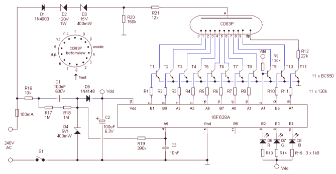
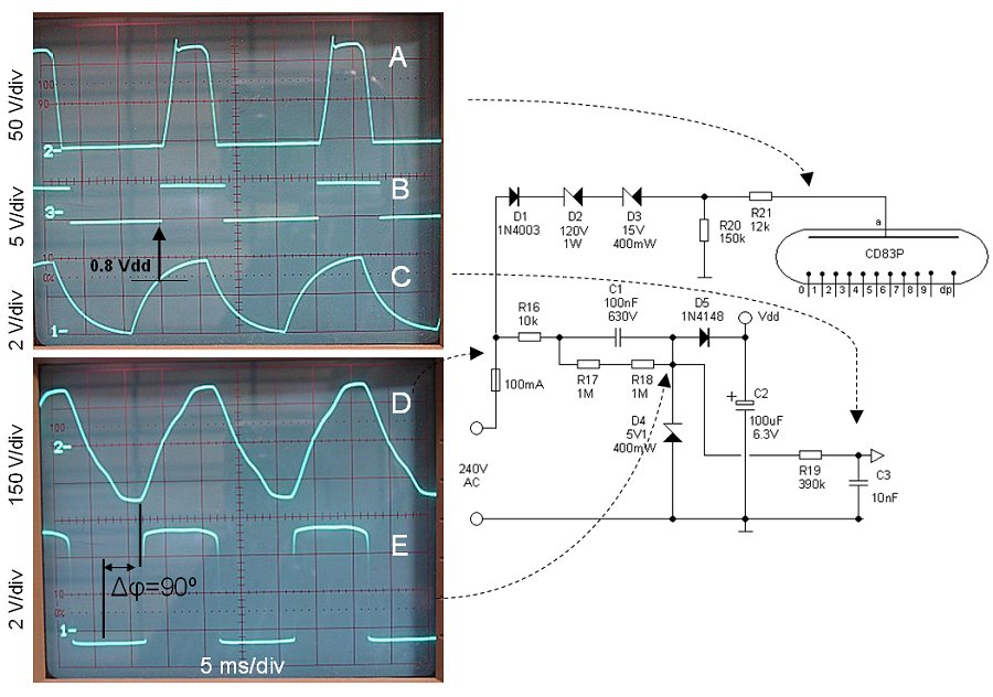
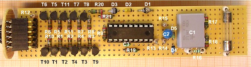
Figure 25 shows the total circuit diagram of the clock. It basically consists of 4 blocks: The low-voltage supply, the high voltage supply, the controller and the nixie plus driver.
The main reason to use discrete transistors to drive the nixie was obviously to demonstrate that it could be done with a standard ōlow-voltageö transistor like the BC550. An additional advantage is that discrete transistors, unlike driver ICs, do not require a supply current. An ordinary 74141 driver requires at least 10-20mA, making a dropper capacitor power supply impractical.
Output A4 of the processor has an ōopen-drainö, so that for this output pull-up resistor R9 was needed. The small area of the decimal point made it burn very bright at the same cathode current as used for the digits. By adding resistor R12 the current and hence the brightness of the decimal-point was reduced to a level corresponding to the digits.
As processor I used the 16F628 PIC microcontroller from Microchip. Since the 50 Hz mains frequency was used for timing of the clock, the processor was configured to run on its internal 4 MHz oscillator, eliminating the need for a resonator or crystal. At a supply voltage of 4.5V and a clock frequency of 4 MHz, the 16F628 consumes something like 0.5mA. Outputs B2, B3 and B4 directly drive the red, yellow and blue LEDs in the ōambilightö three color LED. The total average supply current, including LEDs, amounts to ca. 4mA.
Figure 26 The high- and low-voltage power supplies and its associated waveforms.
The high- and low-voltage supply circuit together with its associated waveforms are shown in Fig. 26. The high voltage supply is basically nothing more than the single sided rectified mains voltage without any smoothing. Zenerdiodes D2 and D3 lower the peak mains voltage to ca. 240V (Fig. 26A), well below the combined breakdown voltage of 270V, of the BC550 and the nixie. Although the nixie tube switches on and off 50 times per second, the eye perceives it continuously on.
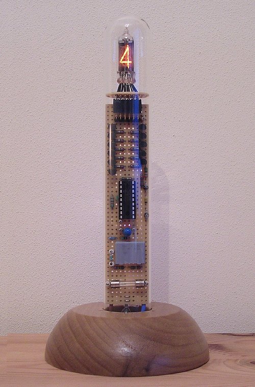
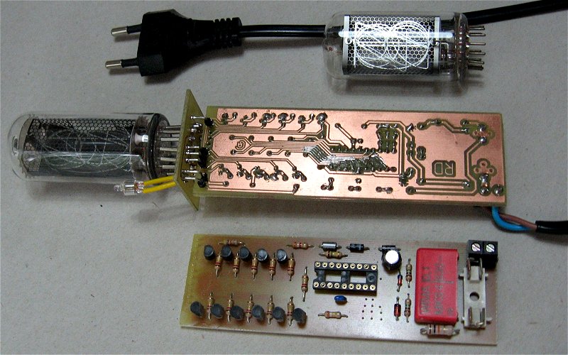
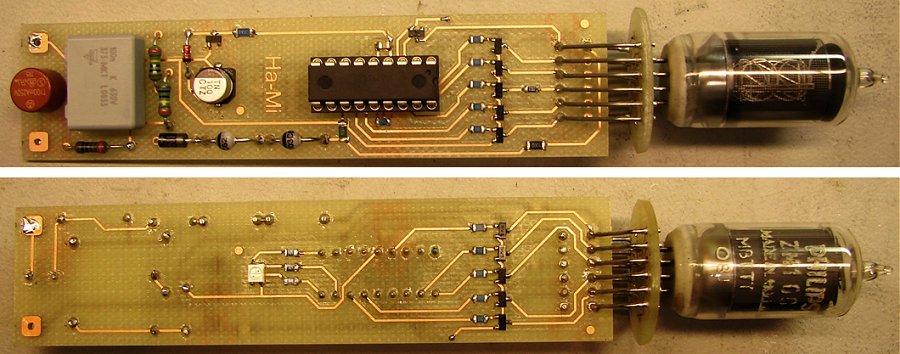
Figure 27 Front- and back-side of the tube-in-tube circuit.
The low-voltage supply is almost identical to the final circuit of the previous section. R17 and R18 have been added to discharge C1 when the clock is switched off. Fig. 26E shows the pulsating DC voltage on the cathode of zenerdiode D4. Note, that the phase of this signal is shifted 90 degrees in phase with the mains voltage (Fig. 26D). The 50Hz clock needed by the processor is derived from the pulsating DC voltage across D4. The low-pass filter consisting of R19 and C3 has been designed to remove, as much as possible, any unwanted transients from this signal. The wafeform after filtering is shown in Fig. 26C. This signal is applied to input A5 of the processor. This is a Schmitt-trigger type input, meaning that the low level input voltage threshold is defined as 0.33*Vdd, while the high level input threshold is at 0.66*Vdd. A small test program which continuously reads the input and copies it to the output was used to test the Schmitt-trigger input. The resulting signal is shown in Fig. 26B.
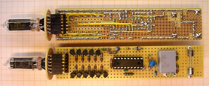
Figure 28 Component placement.
Figures 28 and 29 give an impression how the circuit for the clock was realized. The circuit is so simple that it can easily be built on a piece of breadboard in a few hours. Resistor R16 was mounted in such a way that it is thermally isolated from the PCB and its neighboring components. The reason for this is, that should by any chance capacitor C1 fail, that is breakdown and short-circuit, the complete mains voltage appears over R16. By thermally isolating it, it will become so hot that it will burn down, interrupting the current, without overheating the PCB or other components. The fuse only offers limited protection in such events.
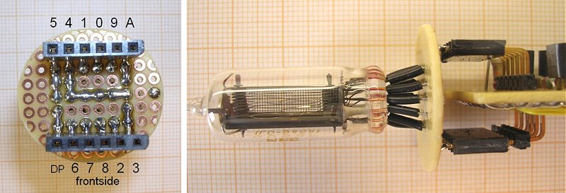
Figure 29 Detail of the nixie tube assembly.
The software
The software for the Tube-in-Tube clock has to simultaneously perform the following tasks:
filter the 50 Hz mains signal
keep track of the time
drive the nixie tube, including on- and off-fading of the digit
process ōthe input keyö
produce a sequence of random colors in the ōambilightö LED
Something which needs a bit of explaining is how the 50Hz mains frequency is used to control three aspects of the clock. The 50Hz obviously is first of all used as a time base for the clock. Although the mains frequency may vary from day to day, depending on the demand of electricity, the owners of the electricity distribution grid make sure that the long term accuracy is guaranteed. Secondly, the on- and off-fading of the digit is, as explained on one of my other pages, realized by phase angle cutting the single-sided rectified mains frequency. This obviously requires synchronization with the mains. Finally, the 50Hz signal, or rather the absence of it, is used to signal a user input.
This obviously needs some explaining. It is a personal aberration, that I hate keys and push-buttons for time adjustment on my clocks. They require wiring which is often ugly and need a hole in the case, which is almost always inconvenient. For this reason I have reduced the number of buttons on most of my clocks already to one. The way it works is very simple; after a reset the clock will scan through all the digits, at second intervals, starting with ōtens of hoursö digit. The digit is fixed by pushing the button. Next the ōunits of hoursö digit starts incrementing, etc. etc. But for this clock even a single digit was too much, first of all simply because I couldnÆt find a place to put it, and secondly because it had to be very good isolated because the entire circuit is connected to the mains. The solution is very simple: to signal an input to the processor, the user simply has to switch the clock off by interrupting the mains power! The buffer capacitor of the low-power supply is large enough to keep the processor working for a number of seconds after switching of the clock, so that it can simply notice the absence of the 50Hz signal it self! The mains can be interrupted by simple removing the plug from the wall outlet (low cost solution), or with a simple mains-cord switch. A neat trick which, as it turns out, works beautifully, and that I undoubtedly will use in many more clocks to come.
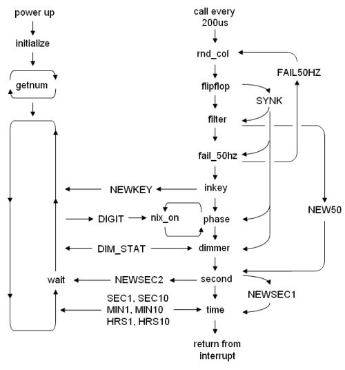
As for most of my clock programs, it consists of a relatively small main program, which is every 200us interrupted by a roll-over from timer 0. The interrupt service routine ōtmrintö in turn calls a sequence of other routines which each performs a time-critical task. These routines communicate with the mains program and the other routines through a set of bits and byte variables.
Figure 30 Tube-in-tube firmware overview.
The left branch represents the main program, the right branch
the interrupt service routine and its components.
Figure 30 schematically depicts the program flow. The left part of the figure represents the main program, while the right part represents the interrupt service routine and its components. The most important variables which are used for communications between different parts of the program have been indicated in capitals. The first part of the program consist of the initialization of the processor (setting of interrupts, configuring timer etc.) and of the program variables. In the next part the time is set in the way described above. Then to program enters an endless loop in which the time is displayed digit by digit. This is done by loading the value of the digit to be displayed in variable ōDIGITö and making ōDIM_STAT=1ö to signal the ōDIMMERö routine, which actually takes care of the on- and off-fading of the nixie, that there is a new digit to be displayed. The main program then uses the wait routine to wait for the beginning of a new second.
As mentioned, the interrupt service routine ōtmrintö is called every 200us. The first subroutine called by ōtmrintö is ōrnd_colö. This routine drives three output pins so as to produce a sequence of random colors on a three color LED. The working of this routine is described else where in great detail. When called every 200us, it functions autonomous with this exception that it will emmediately switch of all three LEDs as soon as bit ōFAIL50HZö becomes set. This bit becomes set is soon as the 50Hz signal is missing. By turning of the LEDs, the current consumption of the circuit is reduced to a minimum, so that the drainage of charge in the buffer capacitor is minimized.
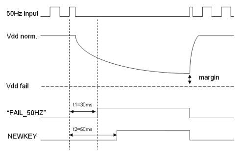
Figure 31 Timing diagram showing how the ōFAIL_50HZö and ōNEWKEYö flags relate to the 50 Hz mains frequency.
The next sub-routine called is ōfilterö. This routine reads the 50 Hz input pin, and removes 90% of the unwanted transients and then sets the ōSYNKö bit in register ōBITSö at the beginning (up going flank) of every new 50Hz period. The ōSYNKö bit is used by many of the other subroutines for mains synchronization. The next two routines, ōfail_50hzö and ōinkeyö, are very similar in function and construction. Both routines detect the absence of the 50Hz signal, only the ōfail_50hzö routine makes flag ōFAIL_50HZö high after 30ms of missing 50Hz signal, while the ōinkeyö routine makes ōNEWKEYö high after 50ms (Fig. 31). The first signal is used to switch of the LEDs, the other to signal a user input. In retrospect, one signal could have been used for both, but when I wrote the routines a had the idea that a much longer time for ōinkeyö to debounce the mains switch would be needed. The routines work very simple. On every call to the routines, they first check if ōSYNKö is set. If so, a new 50Hz period has occurred. In this case a counter is initialized to a certain value n. If ōSYNKö was not set, the counter is decremented. If the counter reaches zero, no 50Hz period has occurred for n*200us. Routine ōfail_50hzö uses a single byte counter while ōinkeyö uses a double-byte counter.
The next two routines, ōphaseö and ōdimmerö, control the on- and off-fading of the nixie tube. Routine ōphaseö performs the actual phase-cutting of the half-wave rectified mains voltage. Depending on the value of variable ōDIM_VALö the tube is turned on a certain fraction of the 50Hz period. When ōDIM_VAL=0ö the tube is off, when ōDIM_VAL=50ö the tube is fully on. Which digit is displayed depends on the value of variable ōDIGITö, which is set by the main program. It is routine ōdimmerö that actually takes care of the on- and off-fading of the tube by increasing and decreasing ōDIM_VALö over time. After the main program has initiated the displaying of a new digit by setting ōDIM_STAT=1ö, the digit fades on and off within one second. The ōphaseö and ōdimmerö routine are explained in one of my other pages . Routine ōtimeö finally updates the time every new second. The time is kept in variables ōHRS10ö,öHRS1ö,öMIN10ö,öMIN1ö,öSEC10ö,öSEC1ö.
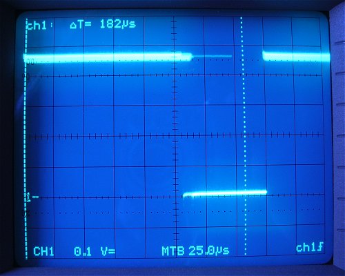
Altogether, this is quite a lot of work for the processor to do within the 200us interval between interrupt calls, especially since the processor is running on the internal 4MHz clock. To verify that the processor is able to finish these tasks before a new interrupt occurs, a simple trick is used. At the beginning of the interrupt service routine bit 5 of PORTB is set, the bit is cleared just before the return from interrupt. By observing PORTB,5 on the scope we get an idea of the duration of the interrupt routine (Fig. 32). Obviously, the length of the routine depends on what needs to be done. From Fig. 32 we learn that the average length of the routine is approximately 135us. However, also longer periods occure. The longest period I could detect is marked by the cursor at 182us, just within the 200us.
Figure 32 PORTB,5 is set high at the beginning of the interrupt service routine, and it is cleared just before the ōreturn from interruptö.
The average length of the interrupt service routine is 135us.
The longest calls recorded measure 182 us.
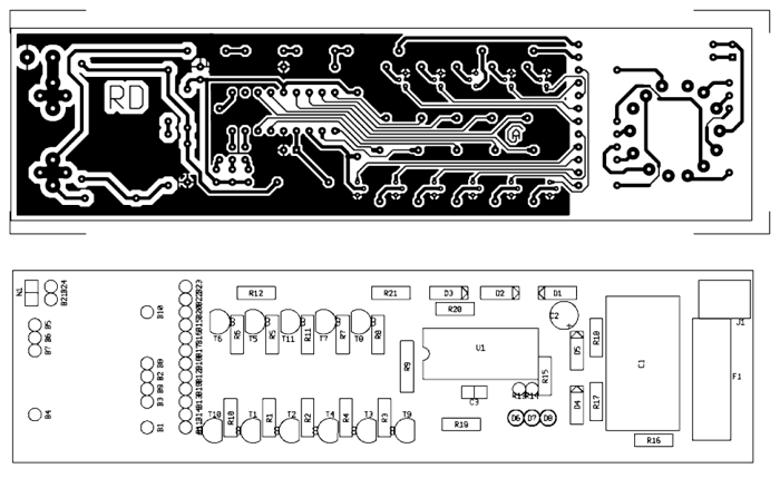
Guus Assmann from Holland built the tube-in-a-tube clock and he created a single layer PCB for it. He was so kind to offer his designs for download on this page. He designed two PCBs one for the IN18 and one for the ZM1020. The last tube has a top view so that the tube can be placed directly on the main PCB. The pins on the connector to the tube PCB are: anode,DP,9,4,5,6,7,1,8,2,3,0.
IMPORTANT!
Both PCBs were designed for MPSA42A transistors! The MPSA42 connections are just the other way around as for the BC550 (CBE for the MPSA42 instead of EBC for the BC550 with the pins up and the flat side towards you). If you want to use this PCB for BC550 transistors, you will have to rotate the transistors 180 degrees! Whatever transistor you use, satisfy yourself that you have mounted the transistor the correct way.
Figure 33 The layout and the component placement of the PCB designed by Guus. Click here or on the picture to download a compressed folder with the artwork for the IN18 and ZM1020 versions.
Figure 34 Impression of the assembled PCB.
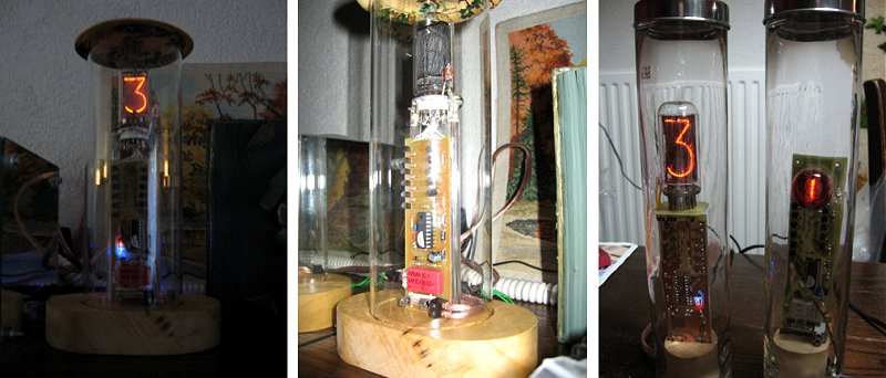
Figure 35 Different Tube-in-Tube clocks made by Guus Assmann.
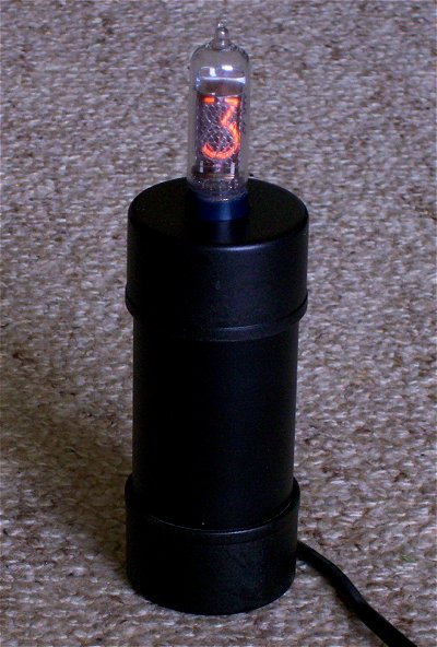
Figure 36 Tube-in-Tube clock made by Herm den Boer.
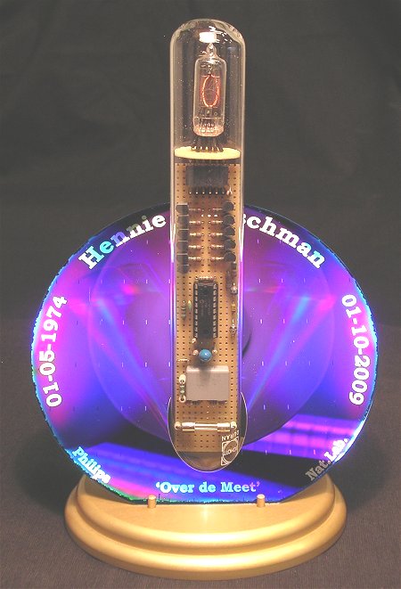
Figure 37 Tube-in-Tube clock for Hennie Kretchman. The silicon wafer has a 0.7 um grating
resulting in a very nice diffraction of the light.
Figure 38 Tube-in-Tube clock made by Hans Michielsen. You can download the artwork he designed in UltiBoard by clicking here. He used the high voltage transistor BF820.
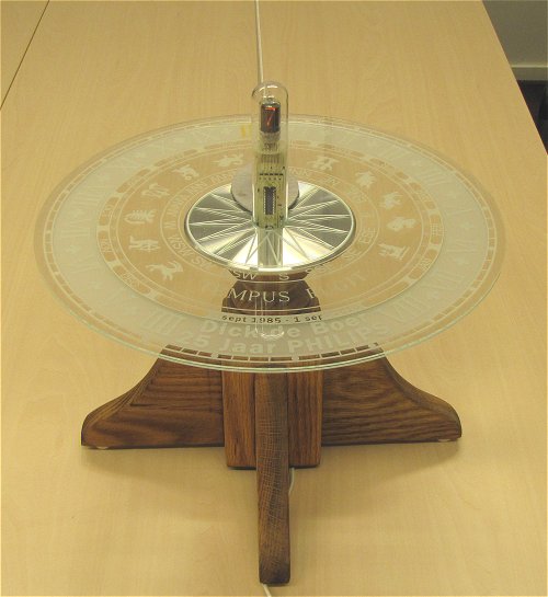
Figure 39 The ōTube-in-Tubeö clock as part of the 25 year jubilee present for Dick de Boer. The text on the sundial reads: ōTempus fugitö (time flees) Dick de Boer, 25 years Philips (Research).

 It is good for a moment to think of what this really means. It means that you have to treat every
part of the circuit as if it is connected to a lethal voltage with respect to ground,
even if the potential differences in the circuit are small! This is sometimes
a little bit difficult for people to understand. I used to have a neighbor who was in the habit
of decorating his garden with Christmas tree lights. Now, instead of buying decent outdoor type
of lights, he used cheap indoor lights. Being a "they don't fool me" type of man, he argued:
I have 40 lights running on 240V so every light only runs on 240/40=6V, which is not dangerous at all.
Despite my repeated arguments, he was unable to see that although the potential difference across
each lamp might be as small as 6V, the potential difference with respect to ground can be as high as
240V. In other words lethal.
It is good for a moment to think of what this really means. It means that you have to treat every
part of the circuit as if it is connected to a lethal voltage with respect to ground,
even if the potential differences in the circuit are small! This is sometimes
a little bit difficult for people to understand. I used to have a neighbor who was in the habit
of decorating his garden with Christmas tree lights. Now, instead of buying decent outdoor type
of lights, he used cheap indoor lights. Being a "they don't fool me" type of man, he argued:
I have 40 lights running on 240V so every light only runs on 240/40=6V, which is not dangerous at all.
Despite my repeated arguments, he was unable to see that although the potential difference across
each lamp might be as small as 6V, the potential difference with respect to ground can be as high as
240V. In other words lethal.
 Instead of making tubes that would run on a
filament voltage of 4 or 6 Volts, they fabricated tubes with a much higher filament voltage so that
when the filaments of all the tubes in a radio were placed in series, they could be directly
connected to the mains. An example of such a radio is the 209U from Philips (
Instead of making tubes that would run on a
filament voltage of 4 or 6 Volts, they fabricated tubes with a much higher filament voltage so that
when the filaments of all the tubes in a radio were placed in series, they could be directly
connected to the mains. An example of such a radio is the 209U from Philips (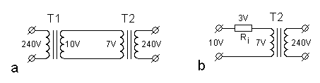
 Since this fifth electron can not be shared with any of the neighboring silicon atoms in the lattice, it is free to move through the crystal lattice. When the electron becomes detached from the dopant atom, it leaves behind the positively charged ion fixed in the lattice, in the figure represented by a ō+ö. Note that the silicon atoms have not been drawn in this figure. When an electric field is applied to the crystal, the free electrons will move in a direction opposite to the field, making the silicon conductive.
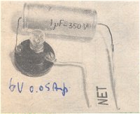 The value of the capacitor is chosen such that its impedance given by 1/(2*pi*f*C) equals the resistance of the dropper resistor that otherwise would have been needed (Fig. 22). The idea is already very old. A dropper capacitor was a favored trick of my father to make a simple low-cost power supply, for instance for trickle chargers. He used to keep a scrap-book with clippings of schematics and pictures of circuits he found interesting or useful and the picture on the left, taken from ōRadio Bulletinö was certainly one of them.
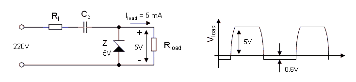
