Some readers of this page have asked me if I could turn this project (the simpler version) into a kit, including PCB. I would like to get an idea how many people would like to buy such a kit. The price would be ca. 30-40 euro excl. shipment. If you would consider buying such a kit, please send me an email
This page describes several circuits which convert a 6V battery voltage to 90V to replace the anode battery in battery operated tube radios. The final circuit does not produce any RF interference and has the special feature that it switches itself on and off!
This page is in the first place intended to document this project for myself. Secondly, I want to teach especially young people something about electronics and above all experimenting with it. Nevertheless, this page has become longer than I ever intended. I can imagine that some readers will find the discussion of the many circuit variants confusing, and not altogether that interesting since most of them didn’t work that satisfactory. Those readers are advised to browse through “The Introduction” and “The Grand Plan” sections (immediately below) and then to skip the sections that describe the final circuits. Two versions of the “electronic battery” were designed and tested:

This page starts with a short holiday trip that my wife, the children and I made to the lovely village of Old-Hastings in the spring of 2010. There in an “antiques” shop in Courthouse Street, I bought a delightful Pye P87BQ portable battery tube radio. A radio like that had been my dream for years, and here it was waiting for me for only 15 pounds! Apart from the fact that the back cover was missing, both the case and the interior of the radio were in pretty good condition. After a thorough clean and replacing several capacitors the set is now in perfect working order again.
My Pye radio is typical for many portable tube radios of that period which all require a 90 V plate- and a 1.5 V filament-battery. It is hard to believe now, but for many decades high voltage batteries were used to power the anodes of radio’s. The very first radio’s in the twenties with directly heated filaments all used high voltage battery blocks and a 4 V lead-acid battery for the filaments. After the indirectly heated filament tubes were developed, mains operated radio sets took the overhand. After the war there was a short revival of battery-powered receivers triggered by the development of several line-ups of very power efficient radio tubes in miniature envelopes. Very well known in Europe are the Philips/Mullard DK92, DF91, DAF91, DL92, DL94 series and its successor, the DK96, DF96, DAF96, DL96 series. This last series made it possible to make a radio which operated at 125 mA (1.5 V) filament- and 10 mA (90 V) anode-current.

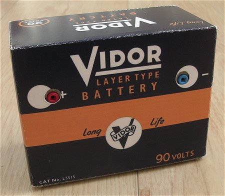
Figure 1.1 A selection of Plate/Anode batteries from the fifties-sixties [1].
Especially the high voltage batteries pose a problem to all those enthusiasts who want to collect and restore these portable radios to their authentic state as close as possible [ 2, 3, 4]. Since these batteries are no longer being manufactured, it is necessary to find an alternative high voltage source. One obvious solution is built a simple power supply that uses a transformer to step down the mains voltage to 90 V and 1.5 V respectively. On the web I have found at least one site which describes such a circuit [5]. Such a solution is however hardly authentic since it turns a portable receiver into maisn operated set.
Not surprisingly, enthusiasts have been looking for truly portable solutions. One popular solution is to take a carton box and fill it with sixty 1.5 V “AA” or “AAA” cells, or ten 9 V packs in series. An example of such a solution is given here. In fact it is not a bad solution at all, IKEA sells ten “AA” cells for 2 euro. These cells have a capacity of ca. 3000 mAh so that at 10 mA plate current you can for 12 euro enjoy your set for 300 hours. However, sixty
 “AA” cells take up a lot of space. Ten 9 V batteries take up less space, but are more expensive (20 euro) and have a capacity of only ca. 500 mAh (50 hrs @ 10 mA). To make it as authentic as possible Roberts has collected on his website a large number of high resolution scans of different battery boxes, so that it becomes possible to re-create an almost authentically looking battery.
An alternative solution is to use a DC-DC converter in combination with a rechargeable battery pack. At first sight this sounds very attractive. There is a wealth of boost- and Flyback-converter IC on the market which make it possible to realize very small and very efficient DC-DC converters which in combination with a small rechargeable NiMH battery Pack will result in a small and sustainable solution. The idea obviously has already been pursued by several authors, but it has one notorious problem. Most of these converters operate at a frequency of at least ten’s of kHz up to a MHz or so, generating harmonics which will directly overlay with the AM frequency band. To suppress these unwanted Electro-Magnetic Interference (EMI) it will be necessary to case these circuits in a shielded metal box on top of a vigorous filtering of the output voltage.
This drawback is overcome by other authors, who use a standard power-inverter topography, operating at 50Hz [
8, 9].
This solution has the drawback that it requires a somewhat larger transformer, but has the advantage that in the AM frequency band the harmonics of the 50 Hz have been attenuated to such an extent that they don’t cause any interference anymore. Considering all the pros and cons I decided to have a go at this type of converter. I think I have a very nice idea to us a small PIC micro-controller to perform most of the functions, including automatic on/off switching, battery control and output voltage regulation. Rather than first finishing the complete project and then write a complete page on it, I decided - just as with my Decatron Clock Project or Ring Counter Page - to write this page in a weblog form, so that I will add chapters as the project progresses. So check this page out from time to time if you are interested in the progress of the project.
| to top of page | back to homepage |
The problem with all inverter-, boost- and flyback converter circuits for electronic batteries I have seen so far is, that even when the radio is turned off, they draw too much current to leave the converter on all the time. The consequence is that the battery needs its own on/off switch, and that you have to “turn the battery on” before you can turn the radio on, which is neither realistic, nor convenient. One solution is to make some additional wiring from the converter circuit to the on/off switch of the radio, but that would also spoil the authenticity. Te nicest solution would be a battery circuit that could detect if the radio is switched on and off. Although at the moment of writing these words, the circuit has not been built yet, I think that it is possible. In the remainder of this section I will try to explain the idea.
The left part of Fig. 2.1 depicts the concept of the electronic battery circuit I have in mind, and the right part shows a simplified circuit of the bias circuit of my P87BQ battery tube receiver, but I guess that it is pretty representative for many other battery receivers. Let’s start with the receiver circuit first. The two AF tubes in the P87BQ require a negative grid-bias. Instead of using a third battery, a simple trick is used to generate this negative bias: the total anode current is fed through resistor Rb, and the voltage drop over this resistor is used as negative grid bias. With a typical value of the anode current of 10 mA, and a resistance value of 470 ohm, the grid bias amounts to -4.7 V with respect to ground. It is obvious that this trick only works properly if the plate/anode voltage is adequately decoupled though reservoir capacitor Cres.
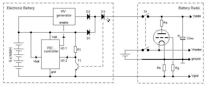
Figure 2.1 Simplified circuit of the electronic battery and the bias circuit of my “P87BQ” receiver.
At the heart of the electronic battery is a PIC micro-controller from Microchip. One of the very interesting features of the PIC processors is that they have a sleep mode in which they consume negligible power. Besides this they have a feature called “interrupt-on-change” which generates an interrupt – which can wake up the processor from sleep – when the logic on a specified I/O pin changes.
Assume for a moment that the processor is in sleep mode and that the high-voltage generator is disabled and also not consuming any power.
When next the radio switch is turned on, Cres will be charged to Vbat resulting in a brief moment of current flowing through D1 and LED D3, which is part of an opto-coupler (1 in Fig.2.1). This will be enough to cause a change on the I/O pin of the PIC processor (2), causing it to “wake up” (3). The processor now knows that the radio must have been switched on, and will turn on the high-voltage, raising the output voltage of the battery through D2 to 90 V (4). As soon as the filaments of the tubes have heated up, a sustained anode current will flow (5) which will turn on the LED in the opto-coupler (6), signaling to the PIC that the radio is in operation. When the radio is switched off again (7), the LED in the opto-coupler will be turned off immediately, signaling to the processor that the radio has been switched off (8) so that the high-voltage can be switched off (9) and that the battery can return to its sleep mode again (11).
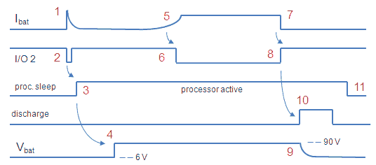
Figure 2.2 Sequence of events taking place in the electronic battery.
There are a few remarks / additions to this plan. The first is that usually at the output of the high-voltage generator we will find a relatively large smoothing capacitor, which will remain charged for a considerable long time after the battery has been switched off and which can give rise to a nasty shock. Even worse it will cause a very high current pulse though opto-coupler LED D3 when the radio is switched on again. To prevent all this, it seems a good idea to add an additional transistor which will discharge the smoothing capacitor after the radio has been turned off (Fig.2.2 (10)).
The second remark is that the processor will be an integral part of the high-voltage generator. As explained in the introduction, I want to use a low frequency power inverter architecture which consists of a transformer and two power transistors which are switched alternatingly. The switching signals for these transistors will be generated by the micro-controller. Furthermore, by changing the duty cycle of the driving signals it is possible to adjust the output voltage depending on the state of the NiMH batteries which can be measured with the AD converter on-board of the PIC controller.
| to top of page | back to homepage |
Most power-inverters consist of two parts: a circuit which converts a DC voltage into an AC voltage, and a transformer which steps up this AC voltage to a high voltage, usually the mains voltage. The basic principle is depicted in Fig.3.1 A and B. In this circuit switches S1-S4 are usually bipolar transistors of power MOSFETs, although also in past also mechanical switches were used. The circuit which controls the switches first closes S1 and S4 and opens S2 and S3. After half a period of the desired inverter frequency, S1 and S4 are opened, and S2 and S3 are closed. Again after half a period, the sequence is repeated, etc. The process creates an alternating magnetic field in the core of the transformer, and the result is that the input voltage is stepped-up by the transformer by a factor equal to the ratio of number of turns on the secondary and primary sides of the transformer.
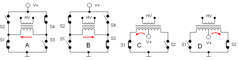
Figure 3.1 Principle of Power-Inverters
If a transformer is used with two identical low voltage turns, the inverter circuit can be significantly simplified (Fig.3.1 C and D). In this circuit each of the two turns generates a magnetic field in the opposite direction so that the current in each turn always has the same direction. This eliminates two pnp or p-MOSFETs and the associated driver circuits. It is this circuit which is used in most power-inverters and also in the electronic-battery discussed on this page. The circuit has another important feature: when both switches are opened the circuit is idle and consumes no power. Additionally by changing the duty-cyle of the on-off switches it is possible to adjust the output voltage of the inverter. A good introduction on inverters can be found here.
Transformers are actually quite complex and tricky elements. Fortunately, there are a number of excellent and comprehensive tutorials on transformers available on the web [ 10, 11, 12, 13]. Let me discuss here the most important features of transformers as far as they are relevant to the electronic-battery project. First of all, an ideal transformer produces an output voltage on the secondary winding which is an exact copy of the input voltage on the primary winding, but multiplied in amplitude with a factor equal to the quotient of the number of turns on the secondary winding and the number of turns on the primary winding. Since power-in must equal power-out, the current scales just inversely proportional. Although most of the time sinusoidal signals are used, this holds for signals with an arbitrary waveform.
Practical inductors however suffer from a number of imperfections such as: inductance, core-saturation and series resistances that we have to cope with in real circuits. First of all practical transformers exhibit an inductance, which limits its use to AC signal. The inductance of a transformer can be measured by connecting only one of the turns of the transformer to a sinusoidal voltage and by carefully measuring the AC voltage and current flowing. The current will be the result of the reactance of the inductor (X = V/I = 2*pi*freq*L). Most of us are familiar with the use of transformers for sinusoidal signals, but what happens if we connect the primary side of the transformer to a square-wave signal as in the case of a power inverter? There are actually two ways of looking at this problem. In the first place a fourier analysis of a square-wave signal learns us that we can consider such a signal as a superposition of a series of harmonics of the sinusoidal fundamental, each with its own amplitude and phase. The transformer will just pass all these sinusoidal signals, so that the square wave signal may be reconstructed at the secondary side. Since the transformer will have the tendency to attenuate higher frequencies, the square-wave signal at the output will have edges which are less steep than in the original signal.
Figure 3.2 Simplified equivalent circuit of a transformer.
The other way of looking at it is in the time-domain. Assume for a moment that the secondary terminal of the transformer is un-connected. When a voltage is applied to the primary terminal of the transformer, the current through the inductance of the transformer will increase linearly according to I=(V/L)*t. With this linearly increasing current, also the magnetic field will increase linearly. Since the voltage induced in an inductor de derivative of the magnetic flux through the inductor, this process will induce a constant voltage in the secondary windings. At a certain moment the core of the transformer will saturate. This means that all magnetic dipoles have now aligned to the field, and the inductance of the inductor will now drop to athe very low value as if it were just an air-core, resulting in a very fast and steep increase in current. It is important that this regime of operation is always avoided since it results in heavy ohmic losses both in transformer as well as in the switches (transistors). Since I=(V/L)*t, saturation can be caused by the applied voltage being too high, or the time that the voltage is applied being too long, for a given inductance of course. When next a load is connected to the secondary winding, a current will flow through the secondary winding, This current is caused from the changing magnetic field. The secondary current draws energy from the magnetic field and will thus weaken it. The reduced magnetic field cannot oppose changes in the primary current as readily as it did before, so the primary winding will draw more current to restore the magnetic field to its full strength.
In a practical transformer all windings also have a resistances. These resistances will cause a voltage drop so that the voltages internally over the “ideal transformer” are less than the voltages applied to the terminals of the transformer. In other words the output voltage is always less than we expected due to resistive losses both at the primary and secondary side. Obviously these resitive losses reduce the efficiency of the inverter.
| to top of page | back to homepage |
Having no experience at all with inverter circuits, I decided to build a test circuit first to get some feeling for these circuits. Since I had the idea to regulate the output voltage by varying the width of the pulses applied to the transformer, it was necessary to also include this feature in the test circuit. The circuit diagram of the test circuit is shown in Fig. 4.1.
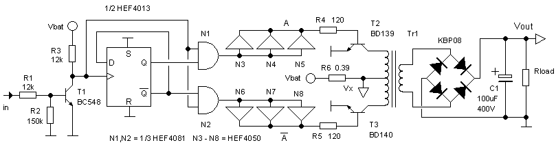
Figure 4.1 The power-inverter test circuit
The input of the circuit is connected to the output of my signal generator with variable duty-cycle control.
Transistor T1 brings the signal levels of the input signal to the supply voltage level of the test inverter circuit: Vbat. Note that T1 additionally inverts the input signal (Fig. 4.3 left). The circuit around the D-flip-flop, which is switched as a toggle flip-flop, and gates N1 and N2 separates the input pulses into the even pulses (A) and odd pulses (A’). Just to be on the safe side, the pulses are buffered with three HEF4050 buffers in parallel, before being applied to the bases of driver transistors T2 and T3. The value of the base resistors is selected so that at the nominal supply voltage of 6V the base current amounts to Ib = (6-0.9)/120 = 42 mA, driving the transistors deep into saturation. Later on the base current can always be decreased. R6 was added to be able to monitor on the scope the collector/transformer current.
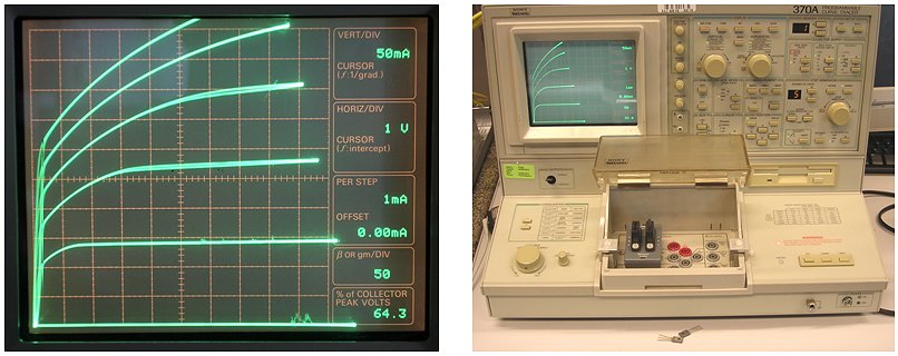
Figure 4.2 IcVce characteristic of a BD139 measured on a 370A Tektronix curve-Tracer.
Figure 4.2 shows an IcVce measurement of a BD139 on a good old 370A Tektronix Curve-Tracer. I wanted to check if up to currents of several hundreds of mA, a simple BD139 still has a sufficiently high hFE to drive it into saturation with a reasonable base current. In the IcVce plot on Fig. 4.2 the collector current is plotted as a function of collector-emitter voltage. For every curve the base current is increased in steps of 1mA, starting at 0 (bottom line) up to 5 mA. We see that for collector currents up to say 300 mA a base current of 5 mA if more than sufficient to drive the transistor into saturation. With this setting for vertical sensitivity and base current stepping, each vertical division also indicates an hFE of 50. So for lower currents the hFE is 150. For currents around 300 mA the hFE due to high injection and/or quasi-saturation decreases to ca. 100, still more than enough for this application.
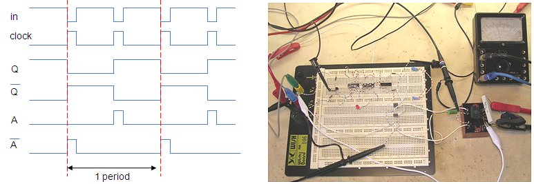
Figure 4.3 Schematic signal waveforms in the inverter test circuit (left) and the actual breadboard circuit (right).
In most power inverter circuits I found on the web power MOSFETs are used to drive the transformer. There are several reasons why I used bipolar transistors. The first and most down-to-earth reason is that I have a whole box full of bipolar transistors, and only a handful of MOSFETs, and personally I think there is a charm in trying to make something with the stuff you just have lying around. The second reason is that - in my experience – MOSFETs tend to die more easily than bipolar transistors. In experimenting with flyback- and boostconverters, I found that the smallest mistake often resulted in the death of the MOSFET. Finally, most MOSFETs require quite a high gate voltage to drive them fully into their low resistance regime, and since I had it in mind to drive the output transistors from a PIC controller running at 3V, this would pose a problem.
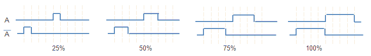
Figure 4.4 The definition of duty-cycle for the power transistor drive signals used in this project.
As explained I want to adjust the duty-cycle of the square-wave signal to adjust the output voltage depending on the state of the battery. For normal square-wave signals the definition of duty-cycle is straight forward. I have no idea if for a an inverter like this there are conventions in the definition of duty-cycle. In this page I use the convention as depicted in Fig. 4.4. This has the advantage that the duty-cycle corresponds to the duty-cycle of the generator signal. Well, not quite, because of the inverter the duty-cycle of the inverter is 100%-(duty_cycle_of_the_generator). An additional inverter would have solved this, but I just didn’t bother.
Figure 4.5 Some of the transformers that I used in the experiments. The transformer finally selected was D.
The first thing I discovered while playing around with this test circuit was that in the performance of the inverter the transformer plays a very important role. Especially some of the smaller transformers I have tried (Fig. 4.5) resulted in a lousy performance in terms of output voltage and efficiency. In Fig. 4.6 I have listed for some of the transformers their nominal design parameters, the primary and secondary winding resistances and the final inverter performance. As a rule of thumb, larger transformers with lower series resistances give a better performance. The transformer I finally selected was a Myrra 44272 which is rated as 2 x 9V with 5 VA per turn, so 10 VA in total. It measures 50 x 42 x 34 mm and weighs about 200 gram. Although this transformer was tested as best in the transformers I had lying around, the losses in the transformer itself are still significant. The total circuit consumed 1.65 W generating exactly 1 W in 10 kohm. From the data in Fig. 4.6 we can calculate that about 0.21 W is dissipated in the transformer.
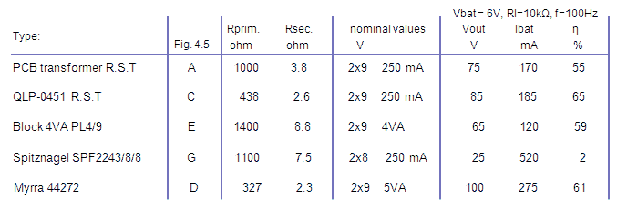
Figure 4.6 Some data on the transformers tested.
Figure 4.7A depicts the base drive signal of T2 (upper trage), Vx which is a measure for the collector/transformer current (middle trace) and the collector potential for T2 (lower trace). The constant negative slope of Vx shows that the current increases linearly to a value of ca 250mA. When T2 is conducting, the voltage drop across it is almost zero, indicating that T2 is fully in saturation as it should be. When T2 is open, the voltage at the collector increases to almost double the supply voltage. The reason is of course that the same voltage which is applied to the primary winding that is conducting, also appears across the winding which is open. Martin Ossman connected both collectors via a diode to a capacitor to generate an additional voltage of 12V this way [9]
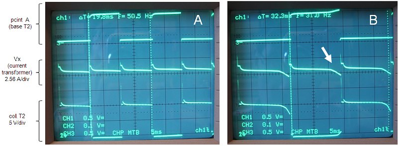
Figure 4.7 Signal waveforms at several points in the test-circuit depicted in Fig. 4.1. In A the core remains unsaturated. In B the current in the transformer reaches the point where the core becomes saturated (white arrow).
In Fig. 4.7B I reduced the frequency a bit to show the effect of core-saturation. At the beginning of each cycle the current starts to increase linearly with time as before, but now – since the cycle time is longer – it reaches a value where are a certain point the core saturates. The white arrow marks this point where the current increases sharply. On the lower trace we also observe that the transistors are pulled out of saturation. This is a dangerous situation since the transistors now conduct a heavy current while at the same time a voltage drop has appeared between collector and emitter. In contrast to the previous situation where they were either conducting current with negligible voltage drop, or were blocking current with a substantial voltage drop ( two situations in which they are not dissipating) in this situation they are dissipating power which can be felt by a sharp increase of temperature.
| to top of page | back to homepage |
The Inverter test circuit proved to be the ideal tool for performing some systematic measurements. In these measurements the supply voltage was varied between 4 V (emulating 5 empty cells 5*0.8 = 4 V) and 7 V (5 full cells 5*1.4 = 7 V) with 6 V the nominal supply voltage. The load of the inverter was varied by connecting different 10W resistors to it: 10k//10k=5k, 10k//15k=6k, 10k, 15k, 10k+10k=20k. From the measured output voltage the output current was calculated.
It turned out to be a bit more favorable to operate the inverter at a somewhat higher frequency. Going from 50 Hz to 100Hz the current drawn at zero load reduced from 111 mA to 67 mA. A somewhat higher frequency also reduces the chance that the transformer is driven into saturation. Most of the experiments in this section have therefore been carried out at 100 Hz.
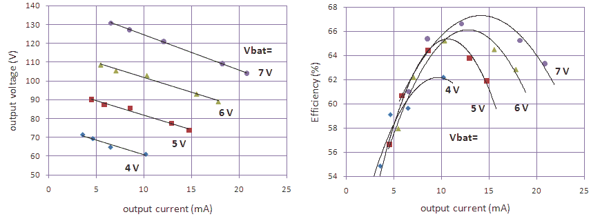
Figure 5.1 Output voltage (left) and efficiency (right) as a function of output current for different supply voltages Vbat.
(freq = 100 Hz, duty-cycle = 95%).
Figure 5.1 shows the output voltage and efficiency of the inverter as a function of output current for different supply voltages. The frequency was 100Hz and the duty-cycle was set to 95% to make sure that the two phases were non-overlapping. The output voltage decreases nearly linear with output load. For the nominal supply voltage of 6 V and the targeted output current of 10mA, the output voltage is a little bit more than the projected 90 V. Furthermore, we find that even for supply voltages down to 4 V – corresponding to five nearly empty NiMH cells – the inverter still produces some 60 V at the output. Since battery receivers were made to operate over a supply voltage range down to 60 V, it means that we can use the electronic battery even for almost empty cells. The efficiency of the inverter does not change that much over output current range and battery voltages (note that the axis only varies between 54% and 68%). The efficiency does however exhibit a maximum which I explained as follows: for low current loads, the losses in the inverter/transformer dominate, for high currents the ohmic losses in the transformer dominate. It should be emphasized again that all these measurements primarily depend on the type of transformer used.
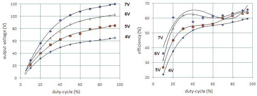
Figure 5.2 Output voltage (left) and efficiency (right) as a function of duty-cycle for different supply voltages Vbat.
(freq = 100 Hz, Rload = 10 kohm).
One of the purposes of the test circuit was to study the behavior of the inverter circuit for different duty-cycles. In Figure 5.2 both the output voltage (left) and the efficiency (right) of the inverter test circuit are shown as a function of duty-cycle as defined in Fig. 4.4 for different supply (battery) voltages and for a frequency of 100 Hz and a nominal load of 10 kohm. Fig. 5.2 shows that by varying the duty-cycle the output voltage can be controlled over a large range. The efficiency remains more or less constant over a wide range of duty-cycles, but shows a sharp decrease for duty-cycles below 40%.

Figure 5.2 Duty-cycle tuned for constant output voltage as a function of battery voltage.
(freq = 100 Hz, Rload = 10 kohm)
In Fig. 5.1 we find that at a duty-cycle of 95% the output voltage of the inverter circuit can vary between 60 and 130 V depending on the state of the NiMH battery. The 12f675 microcontroller I have in mind for the electronic battery has an AD converter on chip, and since it directly generates the driving signals for the power inverter, it seems very attractive to let the micro-controller regulate the output voltage depending on the state of the NiMH cells. For the measurement depicted in Fig. 5.3 the duty-cycle was tuned as a function of different battery voltages for an output voltage of 90 V. Fig. 5.3 (left) shows the duty-cycle and corresponding output voltage as a function of Vbat. For Vbat < 5.5 V an output voltage of 90 V could not be reached even for a duty-cycle of 95%. Fig. 5.3 (right) shows for the same measurement the corresponding input current and inverter efficiency. The measurements were performed at 100 Hz and with a load resistor of 10 kohm.
| to top of page | back to homepage |
‘Do the simplest thing first,’ is a wise lesson somebody (I think it was harrie Maas) once taught me. It is indeed a good advice and I also always teach it my students. In science or technology you can dream up enormously complex solutions or explanations for problems, but most of the time the simplest solution is the best one. A computerized electronic battery is of course very fancy, but looking at the measurement data, one can only conclude that already a simple inverter circuit with a constant duty-cycle of 100% would be very well suited for the job, especially since these battery receivers were designed to be highly intolerant to battery voltage variations.
Figure 6.1 Circuit diagram of the “no-nonsense” electronic battery.
Figure 6.1 shows the circuit diagram of the transistorized electronic anode-plate battery. At the heart of the circuit T1 and T2 form a straightforward astable multivibrator circuit. The values of R5, R6 and C1, C2 have been determined so that the circuit oscillates on a frequency of approximately 100 Hz. Emitter followersT3 and T4 buffer the output signal of the oscillator and provide a low impedance drive source for power transistors T5 and T6. For T1-T4 any equivalent small signal transistor may be used. Also for T5 and T6 any equivalent type rated at 1A, 50V and an hFE of 100-200 may be used.
Figure 6.2 Some basic performance parameters of the “no-nonsense” inverter (Rload).
Figure 6.2 (left) depicts both the output voltage as well as the efficiency of the circuit of Fig. 6.1 for different battery voltages covering the voltage range of a set of 5 NiMH cells (fully charges = 5*1.4=7 V, nearly empty = 5*0.8 = 4V). Even for almost empty NiMH cells the output voltage still exceeds 60V, a voltage on which most battery receivers have been designed to operate. The efficiency over the entire operating range is in excess of a very respectable 60%. The right graph of Fig. 6.2 gives the output voltage and the efficiency both as function of the load current for the nominal battery voltage of 6 V. The performance nearly coincides with the graphs of Fig. 5.1 with a the peak efficiency close to the nominal load current of 10 mA. All-in-all a very descent inverter with a very acceptable performance.
| to top of page | back to homepage |
So far it was only theory, design and measurements on breadboard circuits with “dummy loads.” It now became time to test one of the circuits in a realistic setting, so with batteries and the P87BQ receiver as load. Unfortunately that turned out to be a bit of a disappointment. First of all the hardware - the circuit of Fig. 6.1 - was built on a piece of perfboard, still my favorite way of building circuits.
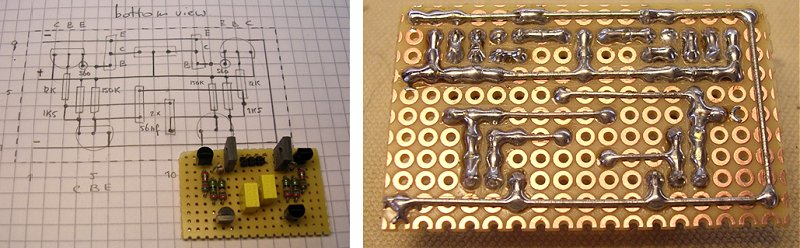
Figure 7.1 The circuit of Fig. 6.1 on a piece of perfboard.
The pictures in this section give an impression of the measurement setup and my “lab-room.” Obviously these pictures give not that much information, but since I like pictures, there they are. From a friend I got ten 4500 mAh Panasonic NiMH batteries. They bare no other marking but that they are development samples. When I received them, the batteries were completely discharged with 0.8 V over the terminals. Not being in a hurry, I charged them with 200 mA for 24 hrs. During the first hour of charging the voltage over the battery rapidly increased to about 1.3 V. During the remainder of the day the voltage very slowly increased to 1.4V. Five NiMH batteries were fixed on a piece of board and the connections to the third and fifth positive terminals were provided with 1 A fuses to protect the battery (and myself) in case I should accidentally short circuit the battery.
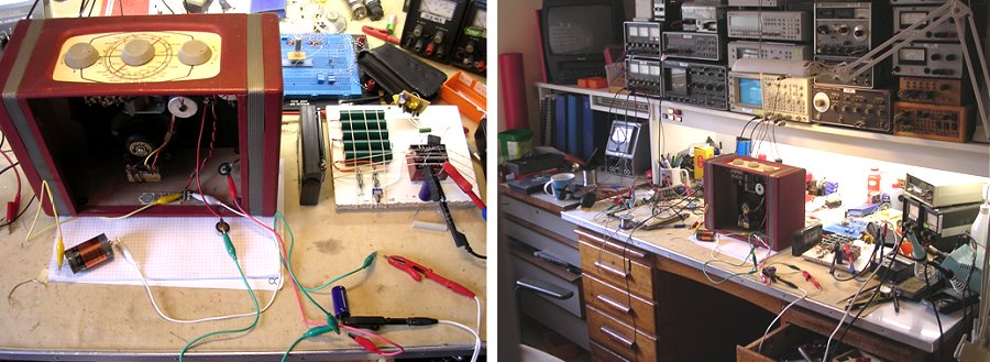
Figure 7.2 Testing of the transistor inverter circuit (left) and an overview of my “laboratory.” Click here for a larger picture.
Not surprisingly the perfboard version of the circuit performed equally well as the breadboard version. However, when I connected it to the PYE radio it produced an incredible 100 Hz rattle! Just to give an impression of how incredible the noise was, I recorded a sample which can be heard by clicking here. By the way, in Holland there are only very few AM stations left. The only stations I can receive are a few very conservative catholic stations, so for those of you who can understand Dutch, my apologies. The origin of the rattle was not clear at first. The article on the 50 Hz electronic battery by Ossman [9], had let me under the impression that the 50 Hz trick perfectly eliminated all noise and interference normally associated with switch-mode power supplies. Apparently either he was mistaken or matters were more complicated.
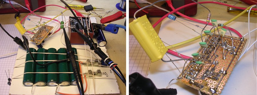
Figure 7.3 Tinkering....
Although I used the basic idea of Ossman, the circuit itself is completely different. Just for the sake of elimination I implemented a few of the features of the circuit from Ossman to see if they would give any improvement. The first thing was to add two flyback diodes parallel to the power transistors. In first order approximation these diodes shouldn’t be needed. Whenever the transistors switch off while there is a current flowing through the primary windings, the energy stored in the transformer should be dumped in the load. However, since the transformer is far from ideal, it will exhibit some stray inductances which can be modeled as parasitic inductances in series with the primary leads. Interruption of currents flowing through these inductances will indeed give rise to transients which may cause interference. Indeed the addition of two diodes parallel to the power transistor reduced the rattle somewhat, but not a lot. The addition of a “snubber” network over the primary windings didn’t give any improvement what-so-ever.
Figure 7.4 Modified circuit of Fig. 6.1 with fly-back diodes and capacitors to reduce the switching speed.
When I put the circuit (including batteries) in a closed metal box (two baking tins from my wife), the circuit was completely quiet. However, as soon as I had one wire coming out of the box the rattle was there again. After some experimenting, the only conclusion could be that the interference was caused by the steep slopes in the current caused by the switching of the transistors. These steep slopes contain high frequency components which apparently continue well into the AM band. By adding small capacitances at the base of the power transistors, it was possible to reduce the slope of the signal. This indeed strongly reduced the 100 Hz rattle. After some experimenting, I found that two 3.3 uF capacitors almost completely eliminated all interference (click here to hear a sample).
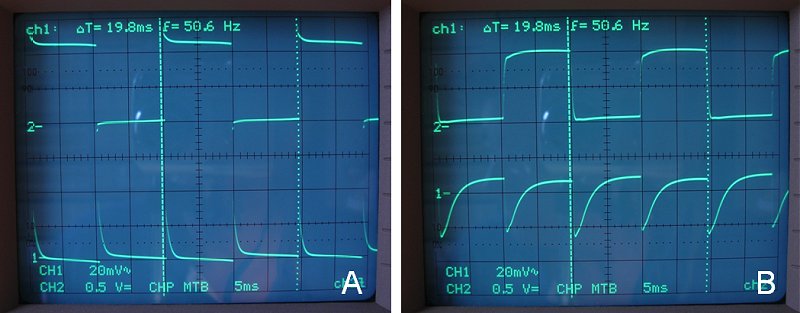
Figure 7.5 Switching wave forms at the primary winding of the transformer (see explanation below).
In Fig. 7.5 the voltage on the collector of the power transistors is depicted on the upper trace (5 V/div), while the lower trace represents the current through the central tap of the transformer, measured at point Vx (Fig. 4.1). When the lower trace drops, the current increases, and when it rises it decreases (0.5 A/div). The left figure is without capacitors. Note the extremely sharp rising and falling edges of the collector voltage. On the lower trace we see that in the transition there is a short moment when there is no current flowing. The right picture is for the circuit of Fig. 7.4 which has the two 3.3 uF capacitors in place. The edges of the signal are less steep, but that comes at a price: at the transition point there is now a moment when one transistor is already turned on, while the other is not yet switched off, resulting in a short peak of almost 1 A in the supply current.
Althought the circuit was quiet now, this current peak increased the average current consumption to 0.67 A, amounting to an overall efficiency of only 18%! Needless to say that the transistors became rather hot. To reduce the switching losses the oscillation frequency was reduced to 50 Hz by increasing C1 and C2 to 86 nF (Fig. 7.3 & 7.4). This only reduced the average current consumption to 0.58 A (η=21%), still a very poor result. At that point I decided that I had seen enough of bipolar transistors for the moment, and that I would try my luck with MOS transistors. When it comes to slow switching, they have intrinsic advantages.
| to top of page | back to homepage |
The gate of a (power) MOSFET can be represented as a capacitance (to ground). The speed by which this capacitance is charged and discharged by the circuit which drives the gate can be easily controlled by adding a series resistance to the gate. In contrast to a bipolar transistor, where the collector current depends exponentionally on the emitter-base voltage, the drain current in a MOSFET is only a relatively weak function of the gate source voltage (linear in the linear region, quadratic in the saturation region). This means that a slow rise of the gate voltage directly translates in a slow rise of the drain current.
The first thing I tried was to replace the bipolar transistors in the test circuit of Fig. 4.1 with two MOSFETs. The only type that I had lying around was a BUK455 from Philips Semiconductors, now NXP. The supply voltage of the driver circuit was increased to 10V, since this MOSFET has - like most power MOSFETs - a rather high VT of several volts. Without additional gate series resistance the test circuit also produced a distinct RFI rattle. This time I didn’t use the PEY to check for any interference, but I just used a simple modern AM receiver. The rattle could easily be picked up by the radio at 30-40 cm distance from the circuit. The noise was strongest in the vicinity of the long wires which connected the breadboard circuit to my power supplies and multi-meters (Fig. 7.2). This made it clear that the final circuit should be as small as possible to avoid radiating antennas. Adding a resistance in series with the gate of the power MOSFETs strongly reduced the 50 Hz rattle. With a gate resistance of 18 kOhm that interference was almost gone.
Figure 8.1 First MOSFET test circuit.
Increasing the rising and fall times of the power transistors at a duty cycle of 100% comes with a penalty. With increasing slopes, the time that both transistors conduct increases, resulting in a strong increase in power consumption and an equal drop in efficiency. In the test setup that was easily remedied by decreasing the duty cycle a bit. The question was if something similar could be achieved in a simple two transistor oscillator circuit like Fig. 6.1. The solution was found by using two diodes and two additional resistors. The principle is shown in Fig. 8.1. Note that when the power transistors are switched off (the gate becomes low), the diodes are conducting so that the gate is discharged through the relatively low resistance resistor of 18 k. When the power transistors are switched on the gate has to be charged through the 750 k resistors which takes considerable more time.
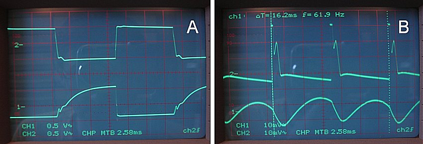
Figure 8.2 Left: signal waveforms at the drain (upper trace) and gate (lower trace) of one of the power transistors (5 V/div).
Right: output signal of the oscillator and the current through the transformer (see text).
The left photograph shows the drain voltage (upper trace) and the gate voltage (lower trace) of one of the power transistors. Clearly visible is that transistor is switched on at a slower rate than off. The result is that the transistor which switches off does this so quick that it is switched off before the other transistor is fully on. The result is a short time in between when both transistors are switched off. Figure 8.2 depicts the original output signal of the oscillator (upper-trace) and the current taken up from the battery by the transformer measured over a series resistance of 0.39 ohm similar to the test circuit of Fig. 4.1. The circuit of Fig. 8.1 works like a dream. At a supply voltage of 6 V it generates 99 V in 10 kohm at a supply current of 275 mA amounting to an efficiency of 60 %.
Although it was (and still is) my aim to make this circuit work controlled by a small PIC processor, I thought it a challenge to see if it was possible to realize the automatic on/off switching functionality with just a few transistors. After some puzzling I arrived at the circuit depicted in Fig. 8.3. The actual power inverter in this circuit is almost identical to the circuit of Fig. 8.1. However, it contains two additions which implement the automatic on/off switching of the circuit, and something which is called a bootstrap which will be explained later on.
Figure 8.3 The complete electronic battery circuit with automatic on/off detection.
As explained before the automatic on/off function is implemented by detecting the small current surge which occurs when the reservoir capacitor in the tube radio is charged when the radio is switched on. The current surge is detected by an LED which is placed in series with the high voltage output of the electronic battery circuit. This high voltage output is connected to an “or” circuit which consists of diodes D7 and D8. As long as the electronic battery is switched off, the output of the circuit is directly connected to the battery through diode D7. So, the output voltage of the circuit is always equal to at least the battery voltage, even when the circuit is turned off. When the circuit is switched on, diode D8 will be conducting, and the output voltage will increase to the inverter output voltage. The LED is part of opto-coupler OC1. So when the radio is switched on, the transistor in OC1 will conduct for a very brief moment.
What is needed next was a timer circuit, which after the small current surge caused by the switching on of the radio, switches the electronic battery on and keeps it going until the filaments have warmed up and the anode current has stabilized. At that moment the LED in the opto-coupler will be on continuously. It had to be a timer circuit which consumes very little, preferably no current, when the timer is in standby because it is on all the time. For a few days I played around with some CMOS circuits from the HEFxxxx series, but I didn’t find it satisfactory or elegant. I wondered if there wasn’t a simpler solution with an implementation only using a few discrete tansistors.
The circuit I eventually came up with was based on
the very well known mono-stable multivibrator topology. The problem with this circuit for this application was that, since one of the transistors is always on, the circuit draws a significant standby current. However, by adding one transistor and a resistor that was easily solved. Figure 8.4 depicts the modified mono-stable multivibrator circuit, or one-shot as it is more commonly referred to. Transistors T1 and T3 form the basic one-shot circuit. Transistor T1 is a phototransistor which is part of the opto-coupler. This circuit makes use of the fact that in the CNY47A opto-coupler also the base of the phototransistor is available on one of the pins of the device. I have to admit that I have never seen a circuit which makes use of this base connection, but this circuit does. So T1 can be switched on by either lighting the LED in the package, or by supplying a base current. Transistor T2 and R2 were added to switch half of the circuit off in standby.
Figure 8.4 Principle of the zero-standby power timer circuit.
Figures 8.4 A-F explain the working of the timer circuit. Let’s assume (we will see later that this assumption is right) that in standby phototransistor T1 is not conducting (Fig 8.4A). In that case the collector of T1 will be at 6 V (assuming a supply voltage of 6 V of course.) With the collector potential of T1 at 6V, the emitter-base voltage of T2 will be zero, so T2 will also be not conducting. As a result the remainder of the circuit will be at 0 V. After some time capacitor C1 will be charged to 6 V with polarity as indicated in the figure. As soon as the capacitor is fully charged there will be no current flowing anymore and we may for sake of DC analysis temporarily remove is from the circuit (Fig. 8.4B). We can now easily reason that since the whole right part of the circuit is at 0 V, the base of T1 will also be at 0 V, and hence T1 will be not conducting. So the circuit is indeed in a stable standby condition.
At a certain moment the base of T1 is exposed to a short light flash because the receiver is switched on (Fig. 8.4C). This will cause T1 to conduct for a fraction of a second. As a consequence the collector potential of T1 will be pulled to zero. This has two effects. First of all T2 will start to conduct powering-up the right part of the circuit. The second effect is that “the anode” of capacitor C1 (it is not customary to talk about an anode in the case of a capacitor, but who cares) will be pulled to ground. Since the voltage over a capacitor cannot change instantaneously, the base potential of T3 will be pulled down to -6 V. With T2 now conducting, and T3 not, the collector potential of T2 will be 6 V. As a result the base of T1 will be biased via R5, so that the circuit will remain in this situation, even if the original light-pulls is over (Fig. 8.4D). It is however a meta-stable condition. What happens is that C1 will be (slowly) discharged through R3 (Fig. 8.4E). As C1 is being discharged, the base potential of T3 will slowly increase from -6 V to 0 V, and then will start being charged to +6 V. However, long before +6 V is reached, T3 will start to conduct when the base voltage reaches approximately 0.8 V. This will cause T3 to conduct. As a result the collector of T3 will be pulled to 0 V. We are now back at the point we started from: with the collector of T3 at 0 V, T1 looses its bias and stops conducting, causing T2 to stop conducting. The circuit is now back in the standby condition. After C1 is again charged to 6 V, which will happen rather quickly since R1 is much smaller than R3, there will be practically no current flowing anymore. The only current that can flow will be caused by leakage currents in the transistors (usually very small) and a leakage current through C1. It is therefore important to use a high quality low-leakage tantalum capacitor for C1. The circuit works like a dream, and the current consumption in standby of my version is smaller than 0.1 µA. Note that when the LED in the optocoupler is on all the time, as will be the case when the filaments in the tubes have heated up, the timer will also remain on. The circuit is thus ideal to bridge the interval between turning on the receiver and a steady anode current flow. In the final circuit the oscillator is also powered by T2.
Figure 8.5 Principle of the bootstrap circuit.
One of my original objections against using MOSFETs was that they usually need a rather high gate voltage to drive them into the low resistance regime. Now, it is true that there are modern power MOSFETs which have a low threshold voltage. The FDS6570A from Fairchild is an example. This 20 V MOSFET has at a gate-source voltage of 2.5 V already an on resistance as low as 0.01 ohm. However, I personally like the challenge to just use the stuff that I have lying around, which in this case only included a bunch of BUK455A’s which need something like 6V on the gate to get them really going. This obviously presented a problem since I wanted to use the circuit down to a battery voltage of 4 V corresponding to a nearly empty NiMH cell of 0.8 V, which is obviously too low to turn the MOSFETs decently on. The solution to this problem was, if I may say so, very simple and elegant. It is called “a bootstrap”.
Figure 8.5 shows the basic idea. To understand how it works, we have to expand a bit on what has been said on the working of transformers in the section on On Power-Inverters and Transformers. There I explained that when a constant voltage is applied to the primary winding of a transformer, the current – due to the inductance of the winding - will increase linearly. This in turn will cause a linear increase in magnetic flux through all of the windings. Since the induced voltage is proportional to the derivative of the magnetic flux variation with respect to time, this will result in a constant, but transformed voltage at the secondary side. In the power inverter a “special” type of transformer is used in the sense that it has two primary (low-voltage) windings that have been connected in series. Since the magnetic flux obviously also passes through this second primary winding, also a voltage will be induced here. Since this winding is identical to the other primary winding the voltage will be the same.
The bootstrap circuit makes use of this effect. Figure 8.5A depicts the circuit before one of the transistors has switched on. Three diodes have been added which are all connected with their cathodes to a reservoir capacitor as they used to call it in the olden days. As a result the highest voltage on one of the anodes will charge the capacitor to that potential, while the other diodes will prevent the flow of a current to a point with a lower potential. The voltage of the reservoir capacitor will be used to drive the oscillator and the gates of the MOSFETs. In the initial situation, the capacitor will be charged to the voltage of the battery. When the transistors are switching (Figs 8.5B&C), one of the outer connections of the transformer will be connected to ground alternatingly (the MOSFETs have been replaced by switches here). Observe that when one side of the transformer is connected to ground, the potential on the other –at that moment not connected side – will be raised to 12 V, double the original supply voltage! This is of course due to the effect I have explained in the previous paragraph. Since the outer connections of the transformer are connected to the anodes of the diodes, the reservoir capacitor will also be charged to double the battery voltage.
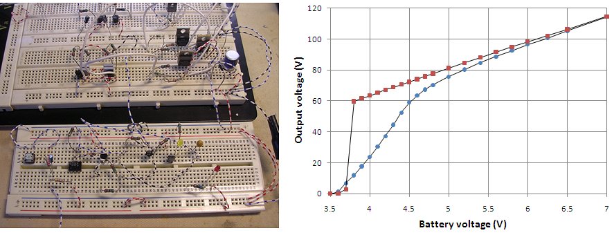
Figure 8.6 The full circuit on breadboard (left), and the output voltage of the circuit as a function of battery voltage
with and without the bootstrap circuit in 10 kohm (right).
In summary what happens is the following. When the circuit is first switched on, the supply voltage of the circuit is only equal to the battery voltage which can worst case be as low as 4 V. At this low voltage the MOSFETs do switch on a bit, but they do not reach their low-resistance on-state. This will cause a voltage drop over the MOSFET and some initial dissipation. However, as long as the voltage drop over the MOSFET is less than half the supply voltage, the voltage on the other side of the transformer will be a bit more than the initial battery voltage. So the next cycle the gate voltage will be a bit higher resulting in a little bit less voltage drop over the MOSFET and a bit higher supply voltage etc. etc. In this way the circuit – like the famous “Baron Munchausen” who pulled himself (and his horse) from the swamp by pulling his own hairs – generates its own supply voltage and after a few cycles the MOSFETs fully switch to their low-resistance on-state.
Figure 8.6 (right) shows the dramatic effect of the simple bootstrap circuit. The line with the circular markers shows the output voltage as a function of battery voltage without the bootstrap circuit, while the square markers show the same measurement with bootstrap circuit. It is important to use Schottky diodes to minimize the forward voltage drop over the diodes. I used a 1A type of Schottky diode at the low currents this circuit operates on such a diode has an almost negligible voltage drop.
| to top of page | back to homepage |
At the end of the previous section is was my plan to copy the circuit from Fig. 8.3 from breadboard (Fig.8.6) to a piece of perfboard, to test it and to conclude that it functioned so well that this was the end of this adventure and that it wouldn’t make much sense to develop a PIC based version. Although I had a nice and compact design for the layout on the perfboard ready (Fig.9.1 right), I decided to first make a breadboard test with the basic inverter circuit on the PQY87QB (Fig.9.1 left).[CT ok! 24-9-2010].
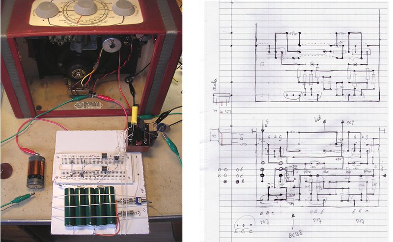
Figure 9.1 Final test of the all-transistor inverter circuit with the PEY87BQ (left) and perfboard design for the circuit depicted in Fig. 8.3 (right).
At first hearing, the inverter sounded pretty ok. Here I have a sample which sounds as good as the sound of any old AM radio recorded with a lousy microphone. But carful listening also revealed a persisting soft but irritating rattle which can be heart in the background of this sample. The noise was especially pronounced on the long-wave band. A lot of experimenting and tinkering was done to find the origin of the rattle. Unfortunately, I was not really able to find the root cause of it, but there were some indications: first of all the rattle increased when I brought my hand in proximity of the oscillator circuit, especially the bases of the transistors. It sounded a bit as if the 50 Hz of the oscillator was interfering with the 50 Hz of the real mains picked-up by my body. It is very well possible that this effect would disappear as soon as the circuit was transferred to a much smaller version on the perfboard. The other fact is that the value of the “snubber capacitor” C5 in Fig. 8.3 is important. Replacing this capacitor by two 2.2 uF electrolytic capacitors back-to-back gave some improvement. Another point of suspicion was the “non-overlapping” driving of the power-transistors with the diode-resistor networks. I have the feeling that it is a design “working on the edge” causing some of the problems especially if there is some phase jitter originating from the oscillator. A design based on a PIC processor would give much more freedom in generating clock signals which are robust. So instead of the perfboard version, I decided to try a PIC based design.
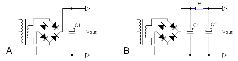
Figure 9.2 Single capacitor (A) and double capacitor / pi network 50 Hz ripple filter (B).
Before doing so this seemed a good moment to look a bit further into the output ripple filter. So far I had used a single 100 uF / 400 V electrolytic capacitor, but was this the most optimal solution? In most vintage circuit diagrams a double capacitor pi-filter is used, with either an inductor or a resistor connecting the capacitors. Martin Ossmann in his design in Elector used a 100 ohm resistor and two electrolytic capacitors of no less than 470 uF / 200 V [9]! Using the transistor inverter circuit on breadboard (Fig. 9.1) and a 10k resistor as load, both the single capacitor as well as the double capacitor filter were evaluated for different component values. The top-to-top output ripple was measured on the scope.
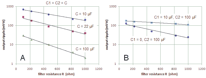
Figure 9.3 Output ripple (top-top in mV) for different component values (see Fig. 9.2).
First the output ripple was measured for different capacitor values in the single capacitor filter. The results were as follows: 100 uF - 200 mV (tt), 22 uF - 700 mV (tt), 44 uF - 400 mV (tt). Next the pi-filter was tested with results presented in the graphs in Fig. 9.3. Since the current at 100 V and 10 kohm was about 10 mA, the voltage drop over the filter resistance increased almost linearly with the resistance from about 1 V at 100 ohm to 10 V at 1000 ohm. Needless to say that with increasing voltage drop the efficiency of the inverter also drops. It is obvious that the pi-filter is much more effective in reducing the ripple than a single capacitor. For the case when C1 = 10 uF and C2 = 100 uF, exchanging the capacitors yielded exactly the same result.
Numbers are very interesting, but what matters in the end is if the ripple is audible. With the PYE receiver connected to the inverter it appeared that a single 100 uF capacitor resulted in a small audible hum which disappeared when a second 100 uF was added (no resistor). With the pi-filer two 22 uF capacitors in combination with a resistor of 560 ohm were enough to remove all audible ripple, a considerable saving in money and space!
| to top of page | back to homepage |
I have to admit that straight from the beginning of this project I have been fascinated by the idea of an inverter circuit directly controlled and driven by a small PIC processor. In the mean time it has become clear how important it is to reduce the switching speed of the power transistors to reduce RF interference. This immediately implies an accurate control over the timing of the switching of these transistors: at all times it should be avoided that both transistors are conducting at the same time, something which can only be realized if these is a sufficient delay between the signals which control the gates of the power transistors. This is obviously an ideal task for a small micro-controller.
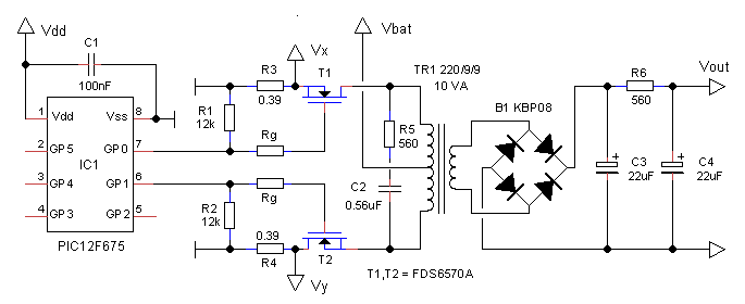
Figure 10.1 First test circuit of the electronic battery circuit controlled by a PIC processor.
Figure 10.1 shows the almost rudimentary circuit used to test the concept. In the circuit I have in mind the PIC controlled is powered by only three NiMH cells corresponding to a supply voltage ranging from 2.4 to 4.2 V. This means that also the gate drive voltages will be in that range. Instead of using a bootstrap circuit like in the previous section, I decided to use a pair of modern FDS6570A MOSFETs with a very low threshold voltage. At a gate voltage of only 2 V the FETs already have an Ron as low as 0.01 ohm. The slope of the switching of the MOSFETs is simply controlled by a single resistor Rg. Two small resistors of 0.39 ohm were included in series with the source in order to be able to directly measure the current through the transistors. Resistors R1 and R2 were added as a safety precaution: when the processor is initializing or when by some other reason the two outputs are in high impedance or input mode, these resistors will pull the gates down, switching of the MOSFETs.
The assembler program which generates the clock signals is very simple (program “bat_1_70.pic” in download “programs.zip”). The processor is configured to run on its internal 4 MHz clock. Timer0 is programmed to generate an interrupt every 500us. When an interrupt has occurred the interrupt service routine sets a flag to signal that an timer0 overflow has occurred. Routine “wait” checks this flag and waits until it has become set, upon which it clears the flag and returns. The main program finally consists of twenty consecutive call to routine “wait” to make up one 50 Hz period (20 x 500 us = 20 ms). The instructions to set and reset the output ports are placed in between the calls to routine “wait” so as to generate the right clock signals.
After some experimenting it was found that a gate resistor of 150k gave an absolutely interference free reception. The whole inverter just worked like a dream. I found it hard to believe after the difficulties with the previous circuits that this one worked so perfect. Although it is difficult to judge the quality of the sound on an imperfect laptop recording, I have included a sound sample here. Note that the recording was made on a Sunday morning that the three strongest stations on the AM band in my area were all three broadcasting a church service at the same time!
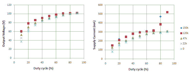
Figure 10.2 Output voltage and supply current as a function of duty-cycle for different gate series resistors (Vbat = 6V, Rload = 10k)
To perform more systematic measurements I programmed a set of ten PIC controllers with duty-cycles in the range of 10% to 100%. I admit that there would have been a more elegant way to vary the duty-cycle then to exchange controllers but I was a bit lazy. In Fig. 10.2 both the output voltage (left) as well as the supply current (right) were measured as a function of duty-cycle for different gate resistances. The output voltage increases with increasing duty-cycle similar to the curve depicted in Fig. 5.2. With increasing gate resistance, the output voltage increases for constant duty-cycle. This can be explained from the fact that with increasing gate resistance the slope of the switching curve decreases so that the energy content of the input signal to the transformer increases. The supply voltage follows exactly the same trend. However, for the the highest gate resistances of 120k and 150k the current sharply increases for duty-cycles larger than 80%. What happens is that for those duty-cycles the one transistor starts to conduct while the other one is not fully switched off yet. A situation which obviously has to be avoided. For a gate resistance of 47k and smaller a 50Hz interference was audible which increased with decreasing resistance.
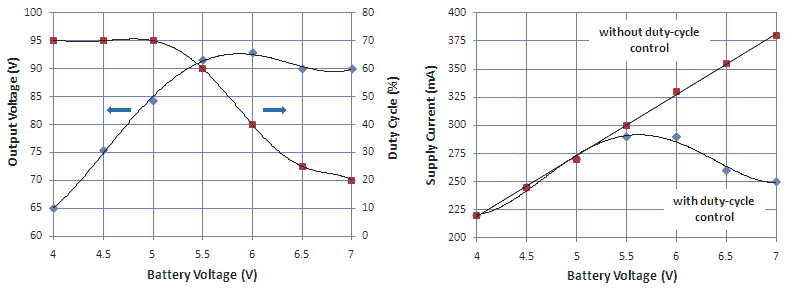
Figure 10.3 Duty-cycle adjusted for constant output voltage of 90V (left) and supply current comparison for the duty-cycle adjusted inverter and the inverter operating with constant duty-cycle of 70% (right). In both cases the load resistor was 10k.
In the measurement depicted in the left graph of Fig. 10.3, the duty cycle was tuned for the expected supply voltage range so that the nominal output voltage of 90V was obtained (if possible at all). For supply voltages of 5V and less the nominal output voltage could not be reached even for the maximum duty-cycle of 70%. The fact that the output voltage is not exactly constant is due to the fact that I had only a limited number of duty-cycle intervals available (the ten PIC processors). In the right curve of Fig. 10.3 the supply current as a function of battery voltage for the circuit in which the duty-cycle is adjusted for a more or less constant output voltage (see left graph), is compared to the situation in which the duty-cycle is kept constant at 70%. In this last case the output voltage increases to over 130V. This waste of power (the radio already works fine at 90V) is reflected in the linear increase in current consumption.
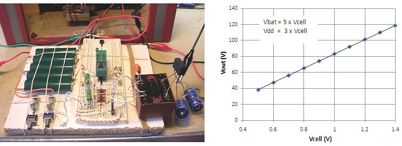
Figure 10.4 PIC inverter test circuit of Fig. 10.1 on breadboard (left) and supply voltage range test (right). The load resistor was 10k.
In the final circuit I have in mind, I am thinking of using 5 NiMH cells in series for feeding the transformer of the circuit while the processor is fed from a tap on the third NiMH cell. This means that when the voltage of a single cell varies between 0.8V and 1.4V, the voltage on the transformer varies between 4.0V and 7.0V while the supply voltage of the processor varies between 2.4V and 4.2V. I was not sure if the processor would work over this supply voltage range and if the power MOSFETs would still properly switch at such a low gate bias. To verify this both the transformer voltage as well as the processor supply voltage were varied as if they were linked to a cell voltage (Fig. 10.4 left). It appeared that the circuit worked reliable for a cell voltage as low as 0.5V. Below this value the oscillator of the processors halts. In other words, the circuit as I have it in mind should work perfect, at least in this respect.
| to top of page | back to homepage |
At a certain point during this project I thought I understood how the inverter circuit really worked. But then, looking at the waveforms in the PIC inverter circuit (especially the voltages at the drains of the MOS transistors), I realized that I was missing a lot of the details which are going on. Time to make a more in depth study of the circuit. As it turned out, things are not really that difficult. With some consequent reasoning a lot can be explained.
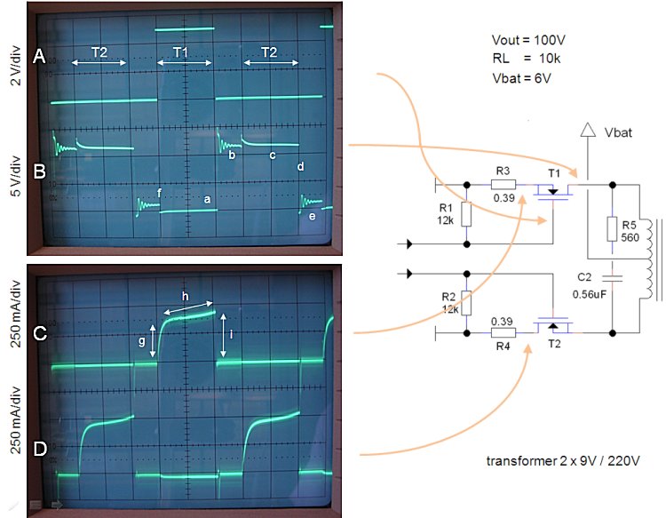
Figure 11.1 Key waveforms in the inverter circuit with Rgate = 0
Figure 11.1 Shows some of the key waveforms in the inverter circuit with the PIC controller. To simplify matters a bit, the gate resistors were removed. This means that the transistors are now switching as almost ideal switches. The PIC generated gate drive signals with a duty cycle of 70%. The upper trace (A) shows the gate drive signal of T2. Note that the processor was running on 5V, while the transformer was connected to 6V. The arrows in trace A shows the moments T1 or T2 is on.
Figure 11.2 Simplified inverter circuit showing the current flow during conduction of T1 (S1)
Lets start simple by looking the shape of the current waveforms. The current through the two driving branches of the inverter are measured indirectly by measuring the voltage drop over two small resisters which were inserted in series with the sources. With the vertical sensitivity of the scope set to 100 mV/div, this is equivalent to a current of I = V/R = 0.1 / 0.39 = 0.256 A/div ≈ 250 mA/div.
Looking at Fig. 11.1 traces C&D, we observe that the current pulses consist of three parts: a jump in current (h), a linear increase for the duration of the pulse (i), and an immediate interruption of the current (j). This behavior of the current can be explained if we replace the transformer by its simplified equivalent circuit consisting of an ideal transformer and a magnetization inductance (Fig. 11.2). An ideal transformer means a component which transforms the voltages and currents on its primary and secondary terminals with a constant ration (220/9 = 25 in this case) for any arbitrary waveforms, even DC signals. The magnetization inductance (Lm) represents - as the word already explains - the magnetization of the metal transformer core. In the model, Lm can be placed at any one of the tree windings. In this case I placed it at the secondary high voltage winding.
When now transistor T1 (represented by switch S1) is closed, a current will start to flow at the primary side of the transformer. How large is that current? Well, when S1 is closed, the battery voltage of 6V is applied to the primary winding. This will instantly cause a voltage on the output of the ideal transformer of 25*6 = 150V. Losses at the primary and secondary side of the circuit reduce this voltage to ca. 100V. The induced voltage on the secondary side causes an immediate current increase through the load resistor, and a linearly increasing current through the magnetization inductance. The current through the load resistor is approximately 100/10k = 10 mA. But 10 mA on the secondary side translates to 25*10 mA = 250 mA at the primary side, which very nicely explains the jump in the current (h). Similarly, the linear increase in current (i) reflects the linear increase of the current in the magnetization inductance. When finally the switch opens again, the current cannot do anything else then to return to zero immediately.
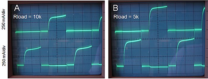
Figure 11.3 Current waveforms for RL = 10k and RL = 5k
By reducing the output load resistor to 5k, the output current is doubled. As can be seen from Fig. 11.3 this naturally results in a doubling of the height of the jump in current, while the linear increase part remains unaffected. If we look carefully, we observe that the linear part shows a kind of an overshoot at the beginning. This is caused by the replenishment of the charge to the buffer capacitor which was lost during the short time both switches were open.
We will now have a look at the shape of the voltage at the drain of T1 (trace B in Fig. 11.1), and we will assume that the output voltage is ca. 100V. Our chain of reasoning starts at point (f) in Fig. 11.1 which corresponds to the moment T1 closes. Since T1 is an almost ideal switch, the voltage on the drain of T1 will be practically zero as long as T1 is closed, represented by part (f-a) in trace B. Although the voltage on the drain is zero during the time that T1 is closed, the current is not and part of the current that is supplied by T1 will – after transformation - flow into the load resistor while another part will be used to “charge” the magnetization inductance as we have discussed in the previous paragraphs.
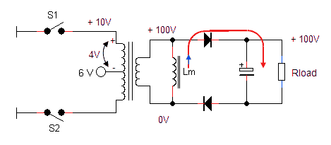
Figure 11.4 Currents and voltages after T1 has opened.
At a certain moment T1 opens (Fig. 11.4). At this point both T1 and T2 are open. What now happens is a bit tricky and closely resembles the working of a flyback converter. At the moment T1 opens, the current in the magnetization inductance has built up to a certain value. We know that the current through an inductor cannot change instantaneously. With both T1 and T2 open, the only way this current can go to is to the load resistor and the buffer capacitor. So what will happen is that the inductor will increase the voltage over its terminals to such a value (ca. 100 + 2*0.8 V) so that the diodes in the bridge will open and it will be able to dump his charge in the output. This voltage will be transformed back to the primary side to a value of ca. 100/25 = 4V. Since the center tab of the primary transformer windings was already on 6V, this means that at the drain of T1 we will measure a voltage of ca. 4+6 = 10V. In trace B (Fig. 11.1) this corresponds to point (b) (forget for a moment the oscillations).
Figure 11.5 Currents and voltages after T2 has closed.
Next transistor T2 is closed. What happens now is exactly the same as when T1 is closed, but since the flux is now pointing into the other direction, the current and voltages on the secondary side are just reversed. What I for the sake of simplicity didn’t mention when we were discussing the situation when T1 was closed, was that the same voltage which is applied to one of the primary windings, obviously also appears over the other primary winding (Fig. 11.5). As a result the voltage on the drain of T1 will now jump to twice the battery voltage, 12V. This effect was used in the bootstrap circuit in one of the previous sections. Since the current is now flowing in the opposite direction on the secondary side of the transformer, the other two diodes of the bridge are now conducting.
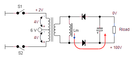
Figure 11.6 Currents and voltages after T2 has opened again.
Finally, when also T2 opens we arrive at the end of the total cycle. Again we have the same situation as when T1 opened, apart from the fact that at the secondary side the currents and potentials are reversed. Again the current through Lm wants to continue flowing. The only way the inductor can achieve this is to raise the potential over its terminal to such a value that the diodes in the bridge will open (100V + 2*0.8V), so that it can dump its charge in the capacitor. The voltage over the secondary terminals of the transformer (ca. 100V) will be transformed down to 100/25 = 4V on the primary side. Since the center tap of the transformer was biased to 6V, this will result in a drain voltage for T1 of 6-4 = 2V (Fig. 11.6). Observe that this rather simple description quite accurately explains the waveform measured on the drain of T2 (Fig. 11.1 trace B).
Figure 11.7 Stray inductances explain the ringing of the drain voltages.
To explain the oscillations in Fig. 11.1 trace B, we have to include the stray inductances present in the transformer. Since in practice the transformer is not ideal, not all the field lines generated by the primary winding are enclosed by the secondary winding. The inductance associated with these field lines can be modeled as small inductances in series with the transformer leads (Fig. 11.7). When the transistor opens, this stray inductance will be “charged”, which together with the drain-source capacitance will cause the ringing observed in Fig. 11.1.
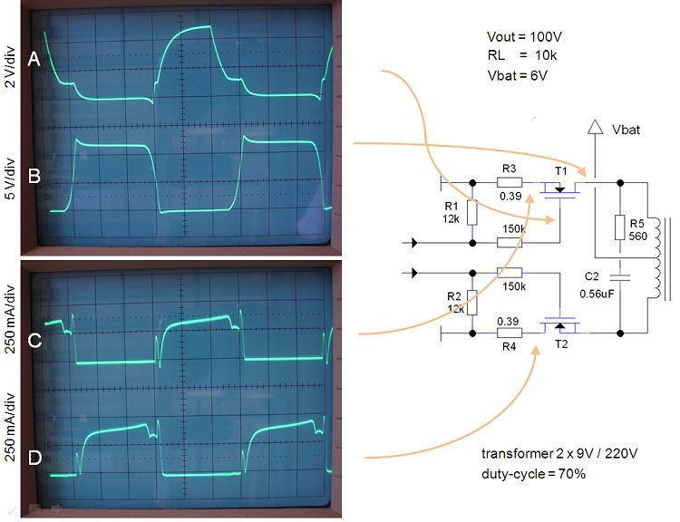
Figure 11.8 Key waveforms in the inverter circuit with Rgate = 150k
When the gate resistances are included, the whole situation becomes a lot more complex. Since the transistors do not shut off immediately anymore, an increasing fraction of the energy stored in the magnetization inductance will be dissipated in the transistors. As a result the circuit will exhibit less “flyback” behavior and will more resemble a transformer circuit which is driven with an ordinary sinusoidal voltage. The spikes in the drain currents are most likely caused by the fact that at 70% duty-cycle the drain currents are still just overlapping.
| to top of page | back to homepage |
I already explained in ”the grand plan” section that it seemed to me a very “cool” idea to measure with the PIC processor the battery voltage, and to adjust the duty-cycle of the inverter circuit for constant output voltage accordingly. As mentioned I plan to use 5 NiMH cells in series with a total nominal output voltage of 5*1.2=6 V. In practice this means that the battery voltage can vary between 5*0.8=4 V for almost empty cells, to 5*1.4=7 V for fully charged ones. From the measurements on the circuit we have seen that for battery voltages less than 5.5V the duty-cycle should be set to maximum (70% to prevent overlapping of the phases) and that even then the output voltage of 90V can not be achieved. In reality this is not such a problem since most portable battery tube receivers were designed to operate on a nearly empty anode battery (60V) anyway. For battery voltages higher than 5.5V regulating the output voltage can give an improvement in efficiency since we can prevent the output voltage from becoming unnecessary high. It should be noted however that only when the battery is fully charged the voltage will increase to 7V. After some discharging the total voltage will rather quickly drop to 6V and remain at that value until the cells are almost drained. So the value of the control system is a bit questionable, but implementing it on the PIC processor seemed fun, so why not?
The 12f675 PIC processor has an on-board 10-bit AD converter, so measuring the battery voltage at first sight seemed to be a no brainer. At second thought things turned out to be more complicated (as they usually tend to do). The AD converter namely does not have an on-board voltage reference, but it uses Vdd as a reference instead. But since I wanted to use a tap on the third NiMH cell to supply the PIC, this meant that the reference voltage for the AD converter would vary just as hard as the battery voltage!
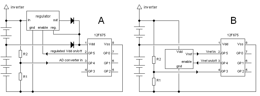
Figure 12.1 Measuring Vbattery the normal way with the variable voltage connected to the input of the AD converter (A), or the alternative way with a constant voltage on the input and the reference connected to the battery (B).
The standard “out-of-the-book” solution would be to use a voltage regulator, preferably a “low-drop” type to regulate the nominal full battery voltage of 6V down to some constant value, say 3V. The problem is that the processor should be able to switch on at any moment, implying that the regulator should also be on all the time. However, since all regulators have a standby power consumption this would “quickly” drain the battery. One solution to this would be to use an unstabilized low voltage derived e.g. from the tap on the 3 MiNH cells during standby, and to switch on the regulated power supply actively (by the processor) only when it is needed (Fig. 12.1A). Another solution would be to use the possibility to configure one of the pins of the 12f675 as a voltage reference input and to connect that to a voltage reference that can be switched on-and-off. I spend some hours dreaming up circuit ideas for one of these two solutions, but in the end they didn’t quite satisfy my taste for simplicity.
Very often you can spend hours trying to solve a certain problem without finding a solution, and then when you turn your thoughts to something completely different, a (or sometimes the) solution pops-up from your sub-conscience. It happens to me constantly in my professional life, and it also happened in this case. My wife and I had spend a weekend in “den Haag” (“the Hague”), and returning by train I had spend the whole journey drawing circuit diagrams of stabilizer circuits. Arriving in Eindhoven (Su 8-8-2010) we got off the train and stepping on the bus it suddenly appeared to me that there are actually two ways of measuring a voltage with an AD-converter. The standard way is of course to supply it with a reference voltage and then to apply the unknown signal to the input of the converter. An alternative way however, is to apply the reference voltage to the input of the converter and to connect unknown volage to the reference input, or in this case the supply voltage (Fig. 12.1B). In both cases the AD converter will return a value which is representative for the unknown voltage and as it happened to be this method was the ideal solution for this particular problem!
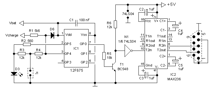
Figure 12.2 Circuit used to test the battery-voltage measurement circuit.
Figure 12.2 depicts the circuit used to test this idea. I used a serial RS232 link to monitor the output of the AD converter. On the 12f765 PIC output GPIO,0 was used for the serial output. Since I wanted to vary the supply voltage of the processor over quite a large range, T1 in combination with N1 were used to translate the varying output signal of the PIC to the standard TTL levels needed for the MAX232. The components to the left of the processor implement the “voltage reference” depicted in Fig. 12.1B. As a voltage reference a simple LED diode was used. An LED has a forward voltage drop of ca. 1.7 V which varies only little with varying current. The anode of the LED is connected with a current limiting series resistance to digital output GPIO,5. So when GPIO,5 becomes high, the LED turns on and the reference voltage is available at analog input AN4. This has the additional advantage that the LED can be used as an indicator light.
The function of R1,R3,R4 and D1 needs a bit of explaining. When jumper J1 is not placed, and when the battery charger is not connected (Vcharge open), the “reference voltage” over the LED is directly connected to the input of the AD converter (AN4) through R3 and R4. When the charger is connected to the electronic battery, Vcharge will be pulled to the charger voltage of 9-12V. R1 together with D1 clamp this voltage to Vdd, so that the analog input will be pulled to Vdd. In this way the processor knows that the charger is connected and that the inverter has to be switched off. When on the other hand jumper J1 is inserted, the analog input will be pulled to Gnd. When this is detected by the processor, the duty-cycle regulation is switched off, and a constant duty-cycle of 70% is used.
A few words on the software used to test this circuit. The test program itself (program “ad.pic” in download “programs.zip”) is very straight forward. Every second it toggles output GPIO,5 so that the LED blinks. At the same time, every second the AD converter samples analog input AN4 so that every first seconds it returns a value representing the voltage over the LED, and every other second it returns zero (unless Vcharge is connected). Only the highest 8 bits of the AD converter are used and they are transmitted as two hex bits in ASCII format over GPIO,0. A small routine is used to implement a software UART (1 startbit, 1 stopbit, no parity, 1200 baud). For this to work correctly, it is important that the internal clock oscillator is “tuned” to 4MHz. Due to fabrication tolerances, it is impossible to make the internal oscillator work at exactly 4 MHz. That is why it is possible to tune this oscillator by adjusting the value of register OSCCAL. The correct value for OSCCAL is for every new processor placed in the highest byte of the program memory in the form of a RETLW (return with literal value in W) instruction. A simple call to this location will return with the correct value for OSCCAL in W. In my case I lost this value, and just adjusted OSCCAL in such a way that the oscillator was running at 4MHz. For this I used a simple test program (program “100hz.pic” in download “programs.zip”) which produces a 100Hz square wave on GPIO,0 when the oscillator is tuned to 4MHz. Note that for every PIC this value differs, so that if you want to use (“ad.pic”) you first have to determine the correct value for OSCCAL, either by using the value supplied by the manufacturer, or by using a short routine like (“100hz.pic”). The delay routines in both programs were dimensioned using the spreadsheet available on my PICdelay page.
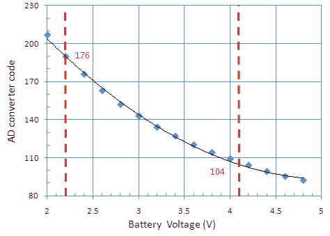
Figure 12.3 Response of the AD converter for varying battery voltage for the circuit depicted in Fig. 12.2.
The graph in Fig. 12.3 shows the AD converter values when the battery voltage was varied between 2 and 4.8V. Note that due to the way we measure Vbat, the AD converter value actually decreases with increasing Vbat. Furthermore the response is somewhat non-linear due to the fact that an LED was used as a voltage reference. Both phenomenons are no problem since still a unique code is assigned to every battery voltage. What can be a problem is that the forward voltage drop over an LED tends to vary a bit from LED to LED, especially from manufacturer to manufacturer. I used a 3 mm very ordinary red LED with a voltage drop of about 1.7V at 1 mA. If you want to build the circuit try to find an LED with approximately the same voltage drop. The highest 8 bits of the AD converter were zero when the jumper was placed. When 9V were connected to Vcharge the AD converter output varied between FC and FF due to some series resistances in the breadboard.
| to top of page | back to homepage |
The final circuit is depicted in Fig. 13.1. The inverter itself is powered by 5 NiMH cells resulting in a nominal supply voltage of 5x1.2V=6V. Since this is too high for the PIC, the power supply for the controller is taken from a tap on the third cell (nom 3.6V). The heart of the inverter circuit consists of transformer TR1, power transistors T1 and T2 and the 12F675 microcontroller IC1. The microcontroller generates the two non-overlapping clock phases with a frequency of 50Hz. The duty-cycle of the clock signal is variable, and depends on the condition of the battery. T1 and T2 are two power MOSFETs with an extremely low Vt so that they can be driven from the controller working on 3V or less. Very essential in the suppression of harmonics which might cause interference at RF frequencies are R8 and R9. These two resistors, in combination with the gate-source capacitances of the MOSFETs increase the turn-on and turn-off times of the MOSFETs. Resistors R6 and R7 ensure that when the processor outputs are in the high-impedance or input state, the MOSFETs are switched off.
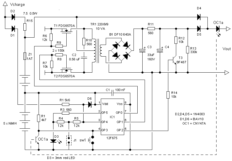
Figure 13.1 Final circuit diagram of the 90V electronic battery circuit.Click here for a pdf version.
At the secondary side of TR1, the high voltage is double-sided rectified by bridge B1 and smoothed by C3, R11 and C4. Listening experiments showed that this filter is quite sufficient to suppress the 100Hz hum. When the battery is switched off, the processor makes output GP2 high for a few seconds. This will make T3 conducting so that the buffer capacitors C3 and C4 are discharged through R12. A simple but effective safety precaution which prevents nasty shocks in experimenting with the circuit after it has been turned off. Resistor R13 provides a minimum load even when the radio is not connected. D4 and D5 form an elementary “OR” circuit. When the inverter is in the off-state, the output will be ca. 5 Volt because it is connected to the battery via D4. When the inverter is on, D5 will be conducting and D4 will block so that the output voltage will be raised to 90V. OC1a is the LED of opto-coupler OC1. The LED senses a flow of current to the radio. This is first of all the short current peak which occurs when the radio is switched on and the buffer capacitor in the radio is charged by the 5V battery voltage which is always present on the output of the battery. The LED additionally senses the anode current (ca. 10mA) when the radio is on. When suddenly the anode current disappears, it signals that the radio has been turned off. The photo-transistor which is the other half of the opto-coupler, relays this information to input GP3 of the processor. When the battery is idle, the program configures this IO in such a way that it “wakes” the processor when a change in logic level on this pin occurs.
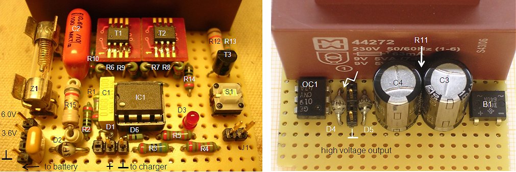
Figure 13.2 Close-up of the final circuit on perfboard
LED D3 serves two purposes: a simple on/off indicator, and a voltage reference. When output GP5 is high, the LED is on with its current limited by R3. The voltage across an LED – or any diode in fact – is only a relatively weak function of the current thought the device, so when the supply voltage of the PIC varies, the voltage over the LED remains more or less constant. GP4 is by the software configured to be the analog input to the AD converter which measures the voltage drop over D3. This input has an high input impedance, so that the voltage drop over R4 and R5 is negligible. The same analog input is used to sense if the charger has been connected to the battery. When a charger with a voltage of 8-10V is connected to the battery, diode will pull the analog input to a high potential whereby the maximum voltage is limited to the supply voltage of the PIC by R1 and D6. So when the software reads an AD value which is more-or-less maximal, it knows that the charger is connected. When jumper J1 is placed, the analog input is 0V (charger not connected). The is a signal for the processor to switch off the automatic duty-cycle control.
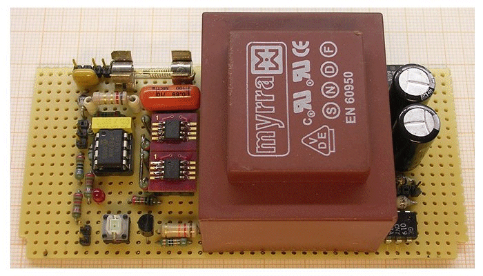
Figure 13.3 Click here for the pdf.
The circuit was built on a piece of perf-board. For me this is always the part of a project I really enjoy. For me it is really a challenge and a game to make the circuit so tidy, neat and beautiful s possible. Hours of planning and drawing with pencil and eraser precede the moment the soldering iron is switched on. For me this is probably as close as I will ever get in producing a work of art. Figures 13.2 and 13.3 give an impression of the final circuit.
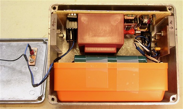
Figure 13.5 The electronic battery circuit in its cast-metal box.
It was more luck than planning that the complete circuit exactly fitted into a 12cm x 9.5cm x 5.7cm
diecast aluminum “Eddystone” box, which also happened to fit exactly in the battery compartment of the PYE radio [10]. The batteries, which were placed in a small plastic box, of the type which are used to organize drawers, together with the circuit fit snugly in the metal box, with only little room to spare (Fig. 13.5).

Figure 13.6 The battery in it’s diecast box and the cardboard box which fits over it.
A large collection of scans of vintage battery packs can be found on Roberts Radio site [3]. The recommended battery for my PYE87BQ was an EverReady B117 of Vidor L5515. The dimension of the diecast metal box differ somewhat from the original dimensions of the L5515 battery, so that the scan had to modified a bit. Of course this is a concession to authenticity, but for me it is close enough. The original L5515 had “Carr Snap Fasteners” of the type which are also used on ordinary 9V batteries, but then larger in size. Since the Fasteners which were on the wires coming from the radio were somewhat corroded I replaced them with miniature “banana” plugs and sockets. The male part was soldered so a small copper disk and isolated with red and black tape so that the final result closely resembles the original. For practical reasons the locations of the banana sockets on the battery had to be moved. Again a small, and in my opinion acceptable, concession to authenticity. A Power-Point file with the layout of the box can be downloaded here.
| to top of page | back to homepage |
At this moment I am still working on the software. I have a version running which implements the oscillator, the automatic on/off feature and the automatic capacitor discharge features. The duty-cycle control still needs to be implemented. Nevertheless, this version of the program works beautifully. The assembler code (battery3.pic) and the associated hex code (BATTERY3.HEX) can be downloaded by clicking here. The full version will come as soon as time permits :-)
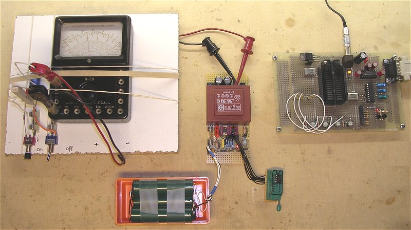
Figure 13.4
| to top of page | back to homepage |
With respect to component count, the electronic battery is pretty compact. The PIC processor takes care of most of the functions, and is ideal to accurately generate the two-phase non-overlapping clock signals for the power MOSFETs. However, for some people the programming of a processor represents an insurmountable obstacle. Most people who love and collect vintage radios have a natural aversion from anything digital, let alone microcontrollers. And I have to confess, when I myself see a circuit using a microcontroller family that I am not familiar with, I do not really feel inclined to pursue it. After some complaints from readers of this page (!) I decided to make “an as simple as possible” version of the electronic battery.
Without the micro-controller obviously some of the features of the battery such as the “automatic capacitor discharge after turn off” and the “automatic duty-cycle regulation” had to be skipped. Fortunately is appeared that the automatic on/off detection could be quite simply implemented. From the exploratory experiments in the previous sections it became clear that if a constant duty-cycle is employed, a 70% duty-cycle is a good choice. Only when the battery is fully charged, the output voltage will be a bit too high resulting in some waste of power, but it will not harm the radio. So for the simplified circuit I opted for constant 70% duty-cycle. What the whole problem now boiled down to, was the question of how such a two phase non-overlapping clock could be generated as simply as possible.
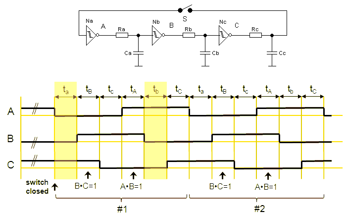
Figure 15.1 Principle of the ring-counter circuit.
The standard solutions for generating the two-phase non overlapping clock signals include the use of an n-bit counter with some clever decoding logic are the cascading of several one-shot multivibrators with a start-up/reset circuit. All these solution require the use of several standard logic ICs. I decided for an unconventional approach by using the good-old ring-oscillator circuit. A ring-oscillator is made by making a loop of an odd number of inverters which will oscillate on a frequency depending on the number of inverters, and the delay per inverter. Usually this is a very high frequency. The oscillation frequency can quite easily be lowered by inserting some extra delays. Figure 15.1 shows this principle. Every inverter output is connected via an RC network to the input of the next inverter. So when an output changes, it will take some time (order of magnitude RC) until the resistor has charged the capacitor to such a value that the input of the next inverter will sense the change in level.
The timing diagram in Fig. 15.1 depicts the voltages A,B,C, on the outputs of inverters Na,Nb,Nc. At the start of the sequence switch S is open. We assume that the input level of inverter Na is low when S is open (not generally the case for CMOS or TTL circuits). The output of Na is high in that case. Assuming that the switch has been open long enough, all capacitors in the circuit will be charged or discharged. In this case it is easy to see that A=high, B=low and C=high. If now switch S is closed, the input of Na will become high because C was high. This will make A low. After some time ta also the input of Nb becomes low etc. etc.
Outputs A,B,C can be considered as the bits a self-advancing counter. The code this counter counts is not a normal binary code. On careful examination we see every new code differs in only one bit from the preceding code. Such a code is called a Gray code. Note that with three bits eight numbers can be represented. The three inverters however go through a complete cycle (indicated in Fig. 15.1 by #1, #2) in six “counts”. Note that codes 000 and 111 are not used.
It was the idea to use a circuit like this to generate the non-overlapping clock signals. Since I wanted to keep the circuit as simple as possible and certainly didn’t want to use a second IC, simple AND gates constructed out of discrete diodes were used to single out two distinctive counts. There are three states which have two bits high (A:B:C 1:1:0 0:1:1 1:0:1). For reasons I will explain later I used the first two combinations.
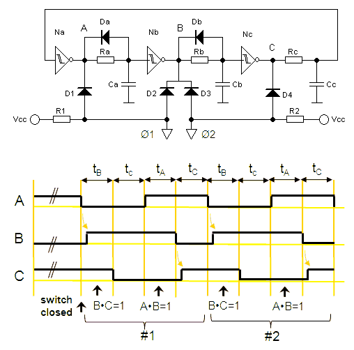
Figure 15.2 The modified ring-counter circuit used to generate the clock phases.
Consider the circuit depicted in Fig. 15.2 and ignore for a moment diodes Da and Db. Diodes D1, D2 and resistor R1 make-up an AND gate which generates the clock signal for the first MOSFET (phi 1). When one of the cathodes of the diodes is low, the output is low. Only when both cathodes are high, the output will be pulled high by the resistor. So phase 1 is high when A=1, B=1, while phase 2 is high when B=1, C=1. The length of phase 1 is equal to tB, the length of phase 2 is equal to tA (note, that tA refers to the time needed to charge capacitor A, while ta refers to the time needed to discharge the capacitor). The spacing between the phases is either tc or tb+tC+ta.
Now comes a trick: if there was a way to eliminate tb and ta then the spacing between the two phases would be determined by tC (and tc). In that case, phase 1 = tB, phase 2 = tA and the spacing = tc = tC. Now as it turns out there is a very simple way to eliminate any state in the complete cycle just by insertion of a simple diode. ta for instance is the time needed to discharge capacitor A with resistor A. Time ta can be reduced to (almost) zero by shunting Ra with diode Da (Note that reversing the diode would have eliminated phase tA). In a similar way diode Db eliminates phase tb. I realize that in words all this sounds a bit complicated, but in reality it is rather simple.
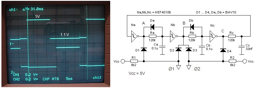
Figure 15.3 Quick and dirty test of the ring-counter circuit.
To test the concept, the clock generator circuit was quickly tested on a breadboard (Fig. 15.3). I didn’t bother to select the components for exact timing. The scope shows the two clock phases as measured with 10:1 attenuating probes (so real sensitivity 2 V/div). As can be seen, the circuit works as expected except for one small thing, and that is that the low level is not really zero but rather 1.2 V. The reason is of course the forward voltage drop of the diodes in the discrete AND gates. For MOSFETs with a somewhat higher VT such as the BUK455 (6V) this shouldn’t be a problem, however for the low VT MOSFET’s the 1.2 V gate voltage will already result in a significant (sub-threshold) drain current.
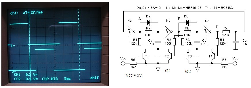
Figure 15.4 basically the same circuit with transistor NOR gates gives a better output low definition.
Figure 15.4 shows an improved version of the ring-counter circuit. Here the two AND gates constructed with diodes have been replaced by two NOR gates constructed with transistors. T1, T2 are just normal npn transistors drawn upside down with emitters grounded and collectors tied to Vcc via the common load resistor R5. When one of the two bases of the transistors is high, the output will be low. The output will be high only when both bases are low (NOR gate). T3, T4 and R6 form the second NOR gate. Referring to Fig. 15.1 states ta (A=0, B=0, C=1) and tb (A=1, B=0, C=0) were selected for phase 1 and 2. In this case tA and tB were eliminated, which was simply done by reversing Da and Db in polarity (Fig. 15.2/15.3). As can be seen the circuit worked like a dream with the low level output now very neatly being pulled to 0V.
| to top of page | back to homepage |
With these clock generator circuits several “electronic battery” power inverter circuits can be constructed. Here I have included the circuit diagrams of two versions. The first circuit uses two somewhat older high Vt MOSFETs, the type of MOSFET that most amateurs are likely to have in their component junk-box, while the other circuit is configured around two state of the art low-Vt transistors. Since the micro-controller version of the circuit already used the low-Vt devices, I decided to only built and test the first version of the “poormans battery” here. At the end of this section the circuit diagram for the low-Vt MOSFET version will be given.
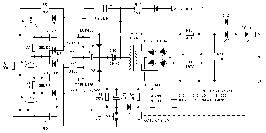
Figure 16.1 The “poormans battery” implemented with high-Vt MOSFETs. Click here for a pdf version.
Figure 16.1 depicts the inverter circuit based on two “high-Vt” BUK455 MOSFET transistors. According the datasheet these MOSFETs have a threshold voltage of about 4 V, but they need a gate voltage of up to 8 V for the lowest on-resistance. The rather high Vt makes is possible to use the simple clock generator circuit with diode AND gates as depicted in Fig. 15.2. To ensure that the circuit also functions reliable at the lower limit of the battery voltage (4V), the bootstrap circuit of Fig. 8.5 was used. In the clock generator circuit Schmitt-trigger NANDS were used instead of inverters. The use of NANDS makes it very simple to power down the oscillator. The spare inputs of the NANDS are all tied together so that when this common input is made low, all the outputs of the NANDS become high. Consequently, when the timing capacitors are all charged, the only current drawn by the circuit is the standby current of the NAND gates, which is very, very low.
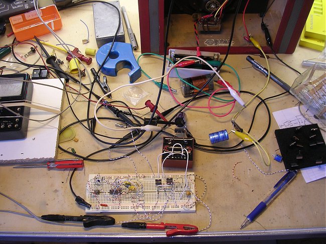
Figure 16.2 Without the need for any programming, the circuit was quickly tested on breadboard.
The power down signal is generated by N4 and opto-coupler OC1. The automatic on/off detection in this “poormans” version of the electronic battery is based on exactly the same principle as the micro-controller version, namely the detection of the charging of the high voltage reservoir capacitor in the radio by the 6V battery voltage which is always present on the output terminals of the electronic battery. So when the radio is switched on, it will cause a short current surge activating the LED in the opto-coupler. As a result the foto-transistor in the opto-coupler will briefly conduct thereby charging C7. This will pull down the input of N4, so that the output of N4 becomes high thereby enabling the clock generator. When the foto-transistors stops conducting, C7 will be discharged through R8 so that after ca. 3 seconds the output of N4 will become low again. However, if during this 3 seconds the radio starts to draw an anode current (because the filaments are heated), the foto-transistor will continue to conduct and the output of N4 will remain high. By pressing S1 the timer circuit can be triggered manually. The power-down (or if you like power-up) signal is also used to power the discrete AND gates through resistors R4 and R5. As a result the gates of the MOSFETs will be automatically pulled to 0V when the circuit is in power-down mode, thereby switching the MOSFETs off.
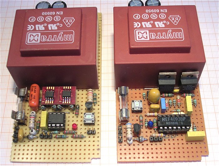
Figure 16.3 The micro-controlled and the “poormans” battery friendly together.
In section 7 it was explained that a reduction of the switching speed of the power MOSFETs is essential for the elimination of 50Hz interference. As in the micro-controller inverter circuit this is done by placing high value resistors R6 and R7 in series with the gates of the MOSFETs. The switching speed is even further reduced by the addition C4 and C5 parallel to the natural gate-source capacitance of the MOSFETs. When the circuit (the HEF4093 and the discrete AND gates) is in standby mode, it is powered from the battery via Schottky diode D10. When the inverter is switched on, diodes D8 and D9 “add” the voltage appearing over the inactive transformer winding to the battery voltage, so that during operation the supply voltage of the circuit increases to almost the double battery voltage. This ensures that the circuit starts swiftly even for battery voltages as low as 4 V. Electrolytic capacitor has to be a high quality type, preferably a tantalum capacitor, since otherwise the leakage current of C6 will dominate the current consumption in standby mode. If this precaution is taken, the standby current is well below 1 uA.
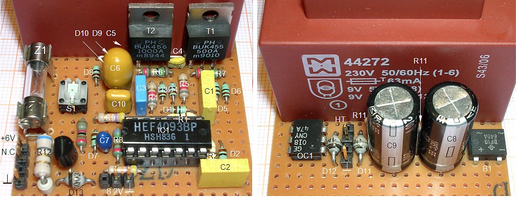
Figure 16.4 Placement of the components. The part numbers refer to Fig. 16.1.
The remainder of the circuit is easily explained. The circuit is powered by a set of 5 NiMH batteries. These particular set of batteries, which have a capacity of 3500 mAh, I got from a colleague who didn’t need them anymore. Although it is not shown in the circuit diagram, the battery is connected to the circuit via a 1A fuse, just for safety. I use an old 8.2V mobile phone charger to recharge the batteries. I didn’t bother implementing some complicated charger circuits, but just used a current limiting resistor. This will charge the batteries at a current of about 120mA, depending on the charge state of the batteries. With such a low charge current it will be difficult to over-charge the batteries. It does however imply that it takes about two days to fully charge the set, but I guess that people who love these vintage radio’s are not in a hurry anyway! It was certainly good enough for me. The 6V battery and the high-voltage output are tied together via an “OR” circuit consisting of D4 and D5. This ensures that even when the circuit is switched off, the output will always be 6V to enable the automatic on/off detection feature. In the final implementation in Fig. 16.4 I added an indicator LED which lights when the battery is on. It consists of a simple npn/LED combination with the base of the transistor connected to the output of gate N4 via a 47k resistor.
The circuit works perfectly without any audible interference or 50Hz hum. The version I built had an efficiency of about 55%. In standby the current drawn from the battery was too low for my equipment to be measured (< 0.1 uA). It can be that when the radio is switched off, the filaments of the tubes cool down so quickly that a considerable amount of charge remains in the high voltage reservoir capacitor in the radio. This might cause an unreliable detection of the switching-on of the radio. The problem is easily remedied by placing a 47k-100k resistor over the reservoir capacitor in the radio. One final word of caution: when the radio is switched off, the smoothing capacitors C8 and C9 will remain charged for some time! Be careful, they might give you a nasty and potentially lethal shock!!
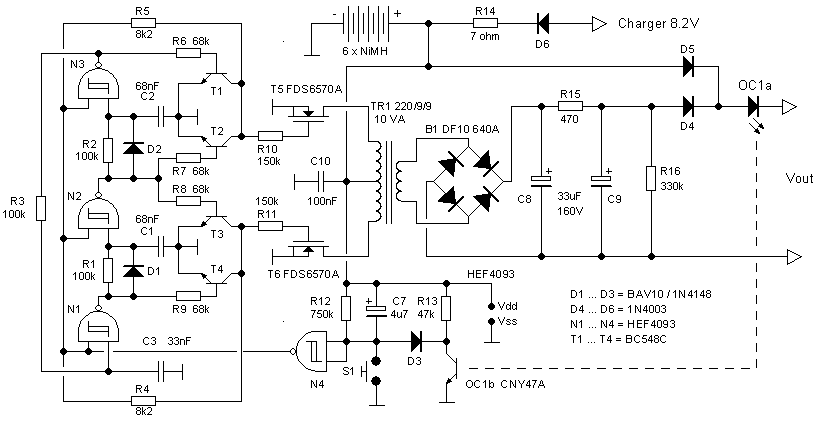
Figure 16.5 Complete circuit diagram of the “poormans” electronic battery with low Vt MOSFET transistors. Click here for a pdf version.
Figure 15.6 finally shows a similar circuit but now designed around two modern low Vt MOSFETs. Just as a warning, this version of the circuit exists only on paper, I didn’t actually built and test it, although I am pretty convinced that it will perform equally well as the other two circuits. Due to the low Vt of the MOSFETs it is not possible to use the same clock generator circuit as in Fig. 16.1. As mentioned in the previous section, the low output voltage of the discrete AND gates is something like 1.2 V due to the forward voltage drop over these diodes. This is too high to turn these low voltage devices completely off. The diodes AND gates were therefore replaced by transistor NOR gates according to Fig. 15.4. Since these MOSFETs are fully on at a gate voltage of 4 V, the bootstrap circuit is not needed in this version of the circuit which represents a minor simplification with respect to the previous circuit.
| to top of page | back to homepage |
A description of the firmware
The filament battery
So stay tuned
Some readers of this page have asked me if I could turn this project (the simpler version) into a kit, including PCB. I would like to get an idea how many people would like to buy such a kit. The price would be ca. 30-40 euro excl. shipment. If you would consider buying such a kit, please send me an email
 |
The 100Hz rattle in the first transistorized version of the circuit using bipolar transistors. |
|
The same circuit, but now somewhat improved by the addition of two slope controlling capacitors. |
|
The first still not perfect circuit which used MOSFETs instead of bipolar transistors. |
|
Detail of the rattle in the same circuit |
|
The perfect sound of the final PIC controlled battery circuit. |
| to top of page | back to homepage |