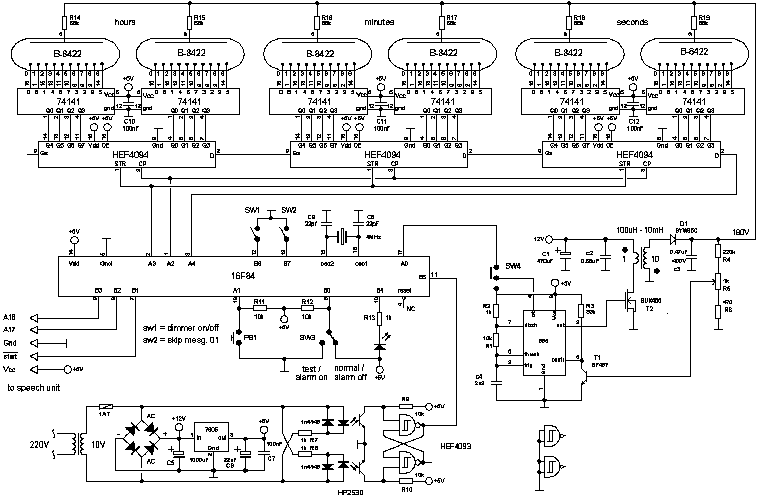
Figure 1. Circuit diagram overview of the NIXIE II clock. Clicking on the figure will open a window with a detailed circuit diagram in pdf format.
When Jim Oostveen gave me a set of Burroughs B8422 Nixie tubes I just knew they were destined to end up in an alarm clock on my bedside cupboard. My house is slowly filling up with homemade clocks, only our bedroom has so far been saved from the "collateral damage" of my clock making mania. A set of romantically glowing nixie tubes will make a big improvement compared to the ordinary twenty year old LED alarm clock I use now.
The B8422 is a lovely "top-view" Nixie tube with a very characteristic semi-rectangular (or semi-round) shape (Fig. 3). This peculiar shape makes it possible to make a row of closely spaced digits e.g. for a calculator read-out, which would have been impossible with a perfectly round top-view type like e.g. the B5031 or ZM1020
For years I have been playing around with the idea of making a talking clock. It seemed to me to be a nice idea to capture the voice of somebody who is special to me, so that I could hear the voice of that person telling the time, even when that person is not there (anymore). EPROMs now have such a large memory capacity that they can easily store a minute or so of audio with quite a reasonable quality. Instead of telling the time I decided to record and store a number of wake-up messages spoken by my sons (Geert 9 and Daan 6). As I am very fond on them, I though that I will wake up a lot more relaxed hearing their voices instead of an angry buzzer.
For the case I want to use the other half of the Plexiglas tube I had left over from the "NIXIE I" clock. The somewhat limited space available in this tube more or less dictated the, at first sight, slightly strange distribution of the clock circuit over the three PCBs. At the writing of this page the final case of this clock was not yet finished. As always I find it the most difficult part of building a clock. When it is ready I will add a picture of the final clock to this page.
I will first describe the circuit of the clock itself (Nixies, drivers,
processor, flyback converter and timebase). Next the realization of these
circuits will be discussed, followed by the speech "generator" which
is a kind of stand alone circuit. The speech, which is stored in an EPROM,
is generated from an ordinary wav file. How this is done will be discussed
in detail. Finally I will summarize the control of the clock and outline
the software. As always all the software used for this clock is available
for downloading at end of this page.
For the heart of the clock I used a 16F84 PIC processor. The 16F84 is no
longer in production, but I had it still lying around. A 16F628, which is
actually cheaper and has more features, is pin and programming compatible,
and will perform equally well.
Figure 1. Circuit diagram overview of the NIXIE II clock. Clicking on the figure will open a window with a detailed circuit diagram in pdf format.
The circuit is to a large extend built up from circuit blocks that I have used in other projects (Fig. 1). The Flyback converter is identical to the one described on the "Flyback Converters for Dummies" page. Since this is an alarm clock we may assume that nobody will read the clock during day-time. To increase the life-time of the tubes the digits are therefore switched of during the daytime. This extends the lifetime of the tube by a factor of two or so. Switching of the tubes is done by completely switching of the Flyback Converter. The easiest way to do that is to pull the reset pin of the 555 low. Jumper switch SW4 has been added to override this feature by directly tying the reset input to +12V (HV on). The 1 Hz timebase is again derived from the 50 Hz mains frequency using the same circuit (and software) as is used in the "LED Clock".
For practical reasons I had to distribute the clock circuits over two PCBs.
To minimize the amount of wirering between the PCBs shift registers were used
to drive the 74141s. The 16F84 does not have enough I/Os to drive all the
74141s directly anyway. Most shift registers that I know of have their
shift register stages directly connected to the output pins. This implies that
during shifting of the data, arbitrary codes are offered to the 71414s,
resulting in artifacts in the display. For this reason I wanted
to use a shift register with an additional output latch. The processor
now first shifts the data into thee shift register, and then copies the
result into the output latches. However, the only 8-bit shift register
with output latch that I had lying around was a CMOS HEF4094. Normally
driving a standard TTL input from a CMOS output in the HEF series is not
considered to be "good practice". Measuring the input currents of the 74141,
it appeared that a logical "1" requires practically no current, will an input
will source 700 uA (for Q0) and 1.5 mA for (Q1,Q2,Q3) for a logical "0".
The HEF4094 outputs are easily capable of sinking these currents, the Vol
level of a HEF4094 output connected to the 74141 inputs was 100 mV for
Q0 and 200 mV for the other inputs, well within the TTL specifications.
Note that this is all at DC levels, and that things will be completely
different when switching speed is an issue.
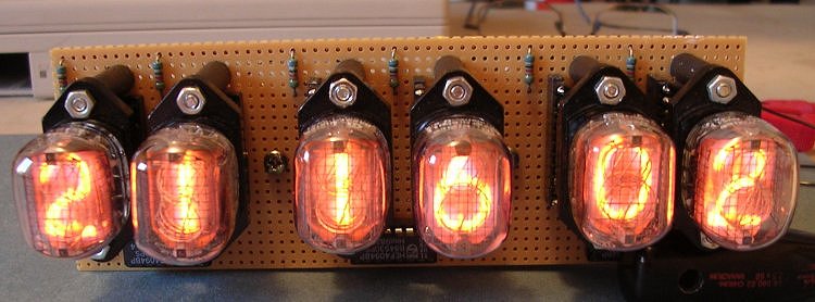
Figure 2. Frontview of the NIXIE II clock. Visible underneath the tubes are the three HEF4094 shift registers, each addressing two digits.
For the construction of the clock, I placed the 74141 drivers directly
underneath the B8422 sockets (Fig. 3d). The socket of the B8422 is a
very special socket indeed (Fig. 3a).
I was fortunate the "Radio Service Twente" in
den Haag has them still on stock for only 1.95 (Euro), as if it was
the most common socket around [1]!
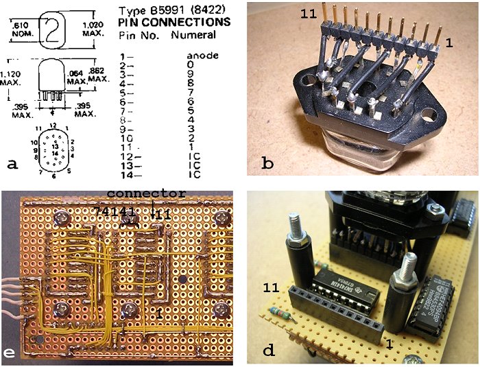
Figure 3. B8422 Construction details: a. pinning of the B8422, b. Connection of the B8422 socket to the "SIL" connector strip (the numbers refer to the connector pin number and not the the B8422 socket pin number), c. Wiring of the "SIL" connector to the 74141, d. Placement of the 74141 underneath the tube socket.
First the B8422 socket is wired to an eleven pin "Single-In-Line" connector strip (Fig. 3b). On side of the socket is directly soldered to the connector strip. Short isolated wires connect the other pins. When inserted into the corresponding female SIL strip, there is just enough space underneath the tube to place a 74141. On the PCB each connector pin is connected to "the nearest" 74141 output (Fig. 3c). Consequently the normal relation between the BCD code and the Nixie digit lit is lost. The processor uses a simple translation table to turn on the proper digit. Figure 2 gives a front view of the clock with all the tubes into place.
| digit | tube pin | connector pin | 74141 output |
| 0 | 2 | 3 | 0 |
| 1 | 11 | 2 | 8 |
| 2 | 10 | 4 | 1 |
| 3 | 9 | 6 | 4 |
| 4 | 8 | 8 | 6 |
| 5 | 7 | 9 | 7 |
| 6 | 6 | 10 | 3 |
| 7 | 5 | 11 | 2 |
| 8 | 4 | 7 | 9 |
| 9 | 3 | 5 | 5 |
| anode | 1 | 1 | N.A. |
The construction of the processor and power supply PCB is very straight forward and hold little surprises. Both PCBs are mounted back-to-back, separated by a sheet of 0.5 mm thick Plexiglas for isolation (Fig. 4). Also visible is the high-voltage output of the converter which is connected with a separate wire/connector to the common anode rail on the display PCB.
All in all a nice and compact assembly which functions pretty well, and fits
into the half Plexiglas tube I have put aside for the case.
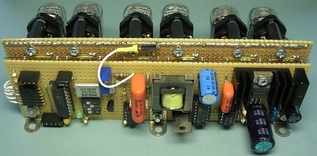
Figure 4. Assembly of the two PCBs back-to-back, and the connection of the high-voltage supply to the common anode rail of the display.
In a wav file the audio signal is stored using either 16 or 8 bits without
any form of data compression (as apposed to e.g. MP3). When you record a
piece of audio e.g. using the Windows Media recorder, you can not
only specify the number of bits, but also the sample frequency. The higher the
sample frequency, the better the sound quality, but the shorter the message
you can store in the EPROM. In this design I have used a sample frequency of
22.050 Hz as a compromise. In the 74C4001 used in this circuit this will store
2E19/22.050=524.288/22.050=23.8 seconds of sound
As a further compromise between quality and
complexity, I use an 8-bit representation. In this case the samples are
stored in the wav file one after another in such a way that 07FH or 080H
represent no signal, and 000H and 0FFH respectively the minimum and maximum
values of the signal in the recording. This is called a binary offset
format.
Figure 5. Circuit diagram of the of the wav file player.
The wav player circuit is basically very simple and breaks down into three functional blocks (Fig. 5). In the first place we have the EPROM holding the wav recording. Secondly, two HEF4040 binary ripple counters are used to step through the EPROM's memory space at a rate of 22.050 increments per second. And finally we have a 8-bit DA converter, a filter and an audio amplifier.
For this project I divided the total memory space of 512 Kbytes into four blocks
of 128 KBytes each. By selecting one of the blocks through A17 and A18 of the EPROM,
the processor can select one of the four wake-up messages stored.
A simple oscillator around Schmitt-trigger nand N4 is designed and
adjusted to oscillate at 44.100 Hz, twice the sample rate. The first output Q0 of
IC2 now toggles at the desired sample rate of 22.050 Hz. This output is used
to clock the data at the output of the EPROM into the AD converter (IC4).
When Q6 of IC1 becomes high the counters have just stepped through an entire
128 KByte memory block. Q6 becoming high will set the flip-flop around N2 and N3.
As a result the HEF4040 counters will be forced in a reset condition, until
a negative going start is issued by the processor. Note that the oscillator
keeps on running all the time.
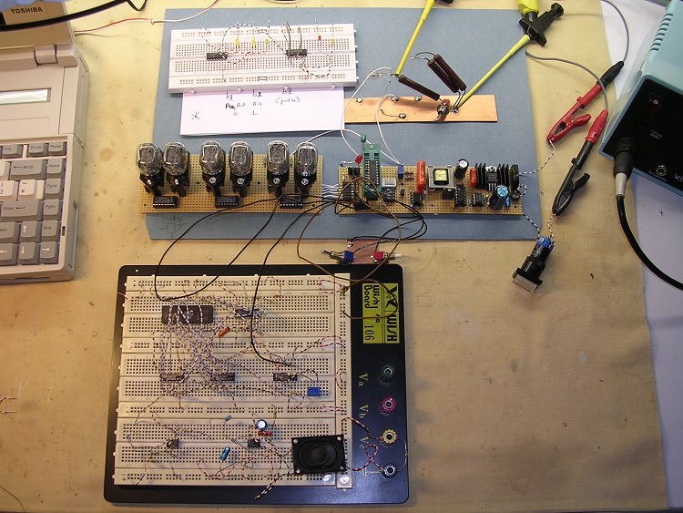
Figure 6. Testing of the wav file player on breadboard.
For the DA converter I used a TDA8702. This is a high speed video DA
converter with an internal data latch. Now I can here you say: "Why on earth
such an obscure component, which possibly not even known on the other side
of the ocean". Well, again the simple reason is that I had a whole bunch of
them lying around, and I make it a sport to re-use discarded or otherwise
surplus components. The advantage of the TDA8702 (apart from the fact that I had
it lying around) is that it has an input data latch. This latch is used to
hold the EPROM output data stable when a carry ripples through the HEF4040s
and the EPROM is internally finding the next
data byte, during which phase arbitrary data may appear at the output, degrading
the signal quality. Most more common DA converters such a the DAC0808 do not
have such a input latch. I have to admit that I am not sure if it is really
necessary. If you want to use the circuit with a different DA converter
I would first test the circuit on breadboard just as I did (Fig.6). If needed
you can insert a separate positive edge triggered latch like a 74HCT274.
A simple low-pass filter removes some of the quantization noise. A MC37071
is used here because of therefore mentioned reason. Any other low-voltage
general purpose op-amp will perform equally well. A very traditional circuit
around an LM386 (IC6) brings the signal to an audio level. The circuit
was built on a tiny piece of breadboard PCB that will be placed together with
a small loudspeaker on the base plate of the case, underneath the tubes (Fig. 7).
To be continued!
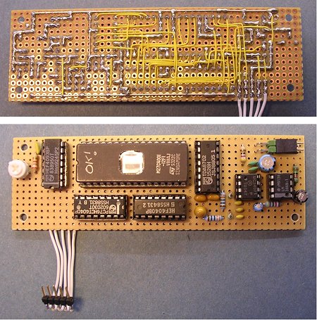
Figure 7. Final construction of the wav file player.
At the bottom of this section you find an actual recording of one of the wakeup messages taken at the loudspeaker and in MP3 format. As you can hear the sound quite reasonable though not perfect because there is still some quantization noise left in the signal. The only way to remove that is to use more elaborate (steeper) filters and/or more bits and a higher sampling rate.

|

|
Basically the steps I follow to come from a wav file (or files) to a programmed EPROM are the following:
The first step is the simplest. I use either the windows media recorder or the "LAPSAudio" wav/mp3 recorder to record the "master" wav file. At this moment we do not want any loss of signal quality so we use a decent sampling rate and 16-bits for this MONO recording. We will sample it down at a later stage. Make sure you record the signal with almost maximum dynamic range, but without clipping.
Next the wav file is trimmed using an audio file editor. I personally use the "Power MP3 editor". So what is there to trim in the wav file? First of all I have always a DC offset in the recorded wav file, which is visible as a shift from the baseline during quiet passages. The only reason that I can think of for this DC offset is the poor quality of my soundcard/microphone. It can easily be removed using the high-pass filter option of the editor, set at a low enough corner frequency (e.g. 10 Hz). Usually the wav file contains some very large peaks during which the signal clips. The peaks are usually caused by burst of air from the mouth hitting the membrane of the microphone. These peaks are cut from the wav file, or reduced in height to an acceptable level. As already mentioned, we want to use the full dynamic range of the DA converter. In other words we want to use all the 256 input codes available. This can be done by amplifying (parts of) the signal. The goal is to obtain a recording in which all the passages have about the same amplitude. Additionally quiet passages may be shortened to cram more text in the EPROM.
This result is saved as the "working wav file", mono, 8 bits resolution at a sample frequency of 22 kHz.
So far, so good. Now we come to a more difficult part. Well, not really difficult, but difficult to explain. Let's start with the wav file. The wav file contains more than just the data samples [2,3]. A wav file starts with a header which is actually quite complex. There are a number of good descriptions of the wav file structure including the header to be found on the internet. However, the only thing we really need to know that the data samples are stored sequentially after the header in 8 bit binary offset format. So if we throw away the first 128 bytes or so, we have stripped the header and are left over with the data samples. This is exactly what I do. I have written a small program (wav.exe) that will read the binary wav file, strip of a certain number of bytes forming the header, and convert the data to an assembler input file containing only DB (Date-Byte) statements. So why not directly generate an INTEL hex file? The answer is that I am lazy. The difficult part of an INTEL hex file is always the checksum at the end of every line. I always have to think very hard how the checksum code is generated. Using the assembler route the assembler takes care of this tricky part.
This leaves only one complication to explain. My EPROM programmer was
designed to only program 27(C)64 EPROMS (8 KByte). A more modern programmer
is still on my "to do list", but drops in ranking every year with the advent
of modern processors with on-board flash. As an intermediate solution I
fabricated an adapter so that my 27C64 programmer will also program
27C256 and 27C4001 EPROMS. These types of EPROMs have more or less the same
programming protocol so that such an adapter is relatively simple (Fig. 8).
The adapter is provided with a series of dip-switches which set the EPROM
addresses beyond the 8 Kbytes page boundary. In this way both the 27C256 and the
27C4001 can be programmed in 8 Kbytes blocks! For this reason the conversion
program splits the original wav file into a series of assembler files with
a predefined size (8 Kbytes in my case).
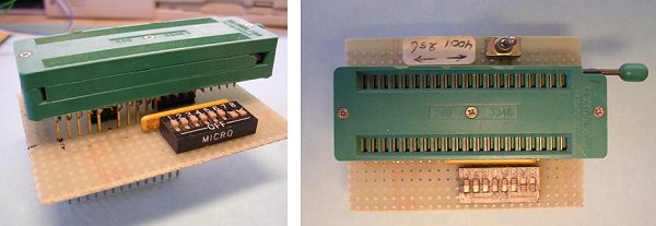
Figure 8. side- and top-view of the 27C256/27C4001 programming adapter.
The conversion program wav.exe was written and compiled in
QuickBasic 4p5 [4] and running under DOS.
In this form it was written to convert a mono, 8 bits, 22 ks/s wav file
with a maximum of 128 Ksamples (131.072 to be specific) into 16, 8 Kbytes
size assembler files. This is enough for a wake-up message of about 6 seconds.
The name of the wav input file should be "working.wav". After start of the
program, it asks for two additional parameters "low" and "high". The parameter
low is the number of bytes which are stripped from the beginning of the wav
file to remove the header. Actually these bytes are not stripped, but
replaced by the value for zero signal (07FH).
Normally I set low to 128 or so. The parameter
high is related to the number of samples in the wav file. Normally, the number
of samples in the wav file will be less than the 131.072 bytes available
in the EPROM. The value high should be set to the number of samples. The EPROM
is filled with the value for zero signal (07FH) for addresses beyond "high".
The source code for "wav.exe", "wav.bas" is very simple and easily adapted
to your specific needs.
The main program of the clock is essentially a state machine. The working and structure of the program is most conveniently described by an explanation of how the clock is operated. This will give an overview of the states the clock can be in, and what the conditions for state transitions are.
The clock is operated through a push-button and a switch. The main function of the switch is switching the alarm on and off. The two positions of the switch are therefore called alarm-on and alarm-off. The first thing the program checks after a power-up (hardware reset) is the position of the alarm switch. If the alarm switch is in the alarm-on position during power-up, the program will enter a test routine: all displays are counted, and everytime the button is pushed the next wake-up message is played (assembler code between labels "test" and "test_2"). When the switch is switched back into the alarm-off position, the clock resumes the normal startup procedure. The normal startup procedure is normally entered when the clock is powered-up with the alarm switch in the off position. The correct time can now be set (assembler code between labels "main_1" and "main_10").
The time is set following the "standard" procedure I use for most of my clocks. After the button is pushed, the hours start counting at a 1 Hz pace. When the button is pushed again, the hours remain fixed, and the minutes start counting. On pushing the button again, the time in the display freezes until the button is pushed for the last time. The clock now starts in normal mode, and we enter state 1.
State 1: show time, alarm not set
State 2: Set Alarm time
State 3: set alarm time.
State 4: Alarm armed.
State 5: Alarm !
State 6: Snooze
The compressed file which can be downloaded here , contains the following files: