

|
|
|
Already from the beginning of the uTracer project, people have objected to the - in the meantime - obsolete RS232 interface. Undoubtedly they have a point, but RS232 is still a very well supported standard, and with a wide choice of RS232-2-USB converters on the market, it is still a very simple and easy interface for all kind of “simple” microcontroller based projects. Nevertheless, it does seem rather superfluous to implement the full RS232 standard including the positive and negative logic levels; conversion from USB to serial using only TTL logic levels also suffices.
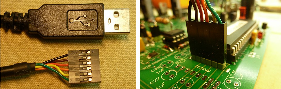
Figure 1.1 Both ends of the TTL-232-5V cable (left), the same cable connected to the uTracer board (right).
The company FDTI (Future Devices Technology International) produces a host of chips that convert the USB protocol to a serial format. However, these chips often use a 3V3 power supply and logic levels. Moreover, they all come in rather difficult to use SMD packages. I experimented a bit with them in the uTracer 4 project, but didn’t find them really easy to use because of afore mentioned reasons. However, recently I bumped into the TTL-232R-5V, a USB to TTL conversion cable made by FDTI that is really easy to use because it does not involve any SMD soldering, and directly interfaces with standard 5 V TTL levels. The cable has on one end a USB connecter which contains the conversion electronics, and on the other end a 6 pin Single in Line (SIL) female connector. By the way, in the same series cables are available that interface to 3V3 logic levels and that have different connectors including a 3 mm Audio Jack. The cable is available from Mouser (part no. 895-TTL-232R-5V) as well as from Farnell (part no. 2419945) and costs about 15 to 20 Euro.
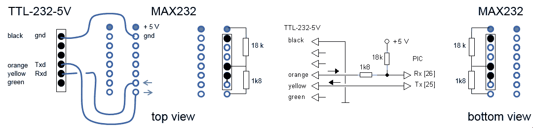
Figure 1.2 Connection of the FDTI cable to the uTracer
It appeared that with some very minor modifications it is possible to directly connect the TTL-232-5V cable to the existing uTracer board. In this way the MAX232, as well as the five 1 uF capacitors can be eliminated. In the first tests with the cable, two problems were encountered. The first problem was that when the cable is directly connected to the processor while the uTracer is off and the cable is connected to a life USB port, the cable will power (a part of) the uTracer circuit causing the power LED to light up. What happens is that a high level on the serial input pin of the PIC will raise the potential on the Vcc bus through the ESD protection diodes in the PIC. To prevent damage to the USB cable a 1k8 series resistor in the receive path was included to limit the current drain on the output of the cable. The second problem that was encountered was that when the cable was not connected to the uTracer board, the floating serial input pin of the PIC caused erratic behavior of the PIC, sometimes resulting in an uncontrolled runaway of the boost converters! The same situation also occurred with the cable connected to the board, but with the USB plug not inserted in the PC. A simple 18k pull-up resistor to Vcc ensures a well-defined potential in the serial input of the PIC and eliminated the problem.
The circuit diagram of the connection to the PIC is shown in Fig. 1.2.
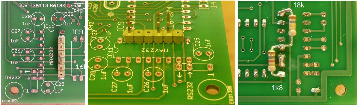
Figure 1.3 Modifications to the uTracer board
The physical implementation of the connection is very simple and elegant. I used a 6 pin male SIL connector from which the not used pins were removed. I always insert these pins in the not used holes of the female part and clip them flush with the edge of the connector. In this way it becomes impossible to insert the connector in the wrong way. The connector was placed on the PCB in the holes intended for the MAX232 in the way shown in Fig. 1.3. On the backside of the PCB a solder bridge connection and two resistors connect the cable connector to the PIC (see Fig. 1.2 and 1.3).
Installing the TTL-232-5V cable was very straight forward. In Windows 7 (as well as 8), when the computer is connected to the internet, it suffices to insert the cable into an USB port after which Windows will automatically download and install the required driver and assigns a COM port to the USB cable. The COM port number used can be found by going to: start > Control Panel > System and Security > Device Manager or Go to Start Menu Search or Run window and type: devmgmt.msc, then expand tab Ports (Com & LPT1). For windows XP it may be necessary to install the drivers manually. Directions for installing the necessary drivers can be found here.
| to top of page | back to the uTracer homepage |
Being under the assumption that most tube lovers are not in a great hurry - the heating and stabilization of a heater takes a minute or so anyway - the circuit of the uTracer has been kept as simple and cheap as possible at the expense of some speed. Having said that, it is always nice to squeeze as much speed out of the circuit as is possible!
Working on another not unrelated project (more on that one another time), the measurement time had become irritatingly long. The measurement time is mainly determined by three factors: the charging time of the reservoir capacitors, the discharging of the capacitors after measurement of a curve, and the communication of the uTracer with the PC. In this particular case the boost converter had to charge a much larger capacitor which resulted in a significantly longer measurement time. Consequently I started looking for a way to “boost the boost converter.”
The power the boost converters can deliver depends on the energy stored in the inductor per cycle, and the number of cycles per second. Assuming that the latter is constant (determined by the firmware), the only solution is to increase the energy stored in the inductor. The energy in turn is proportional by the inductance and the square of the peak current. Unfortunately we cannot increase the peak current in a practical inductor beyond the value where the inductor saturates, or in other words where the core material is magnetized to such an extent that the inductance collapses. This saturation current decreases for increasing inductance so that we have to find an optimum inductance for a given inductor construction (read inductor volume). For the 330 uH inductor used in the uTracer3 the saturation current is about 1 A.
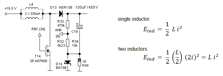
Figure 2.1 Increasing the power of the boost converter by connecting two identical inductors in parallel.
I had already ordered a much larger inductor with a higher saturation current and alas also a much larger foot print when it occurred to me that there is a much more elegant way that is directly compatible with the existing uTracer3 PCB. The idea is to simply connect two inductors in parallel whereby the second inductors is mounted on the backside of the board! Figure 2.1 shows the math. By placing the two 330 uH inductors in parallel the inductance halves, but the peak current doubles and since the power is proportional the square of the peak current, the net result is that the energy stored doubles.
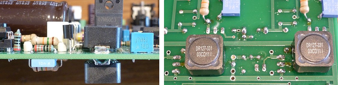
Figure 2.2 Placement of the additional inductors on the backside of the board.
The inductor used is a DR127-331-R from Coiltronics. It is available from Mouser (part no: 704-DR127-331-R), from Farnell (part no: 2075610) or Digikey (part no: 513-1048-2-ND). Figure 2.2 shows how the extra inductors are placed on the backside of the board. This requires a bit of fiddling. In close proximity of the solder pads of the inductors there are a number of other solder points, and it requires some skill to position the backside inductors and solder them. If needed a small spacer in the form of a piece of wire can be helpful to create some distance between the board and the inductor.
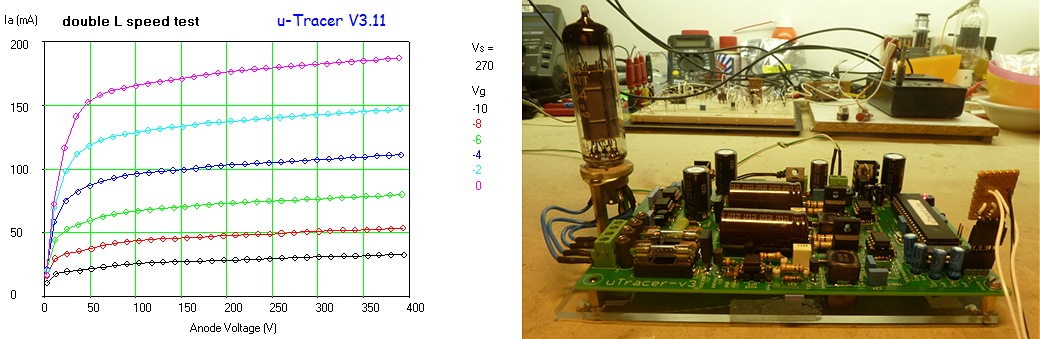
Figure 2.3 Left, measurement used to test the speed increase of the uTracer with the extra inductors; Right, one of the bare uTracer test boards I use to test new circuit and software ideas.
How much speed do we gain? That depends a bit on the type of measurement and the voltage range. The boost converters have to work hardest when the anode and screen voltages are high, so that is where we can expect the gain in performance. Figure 2.2 shows a kind of standard measurement that I used as a bench mark test. With a single inductor the measurement took 2’25”, with the extra inductor this reduced to 1’50”. Not exactly half the time, but still a noticeable improvement, and it may be a good idea to add two of these tiny inductors to the bill of materials the next time you order components from your favorite vendor.
Before people start mailing me, adding a third inductor didn’t bring any substantial improvement. There can be a number of reasons for this: the gate drive of the MOSFETs is too low to carry the additional current, the currents do not distribute evenly over the inductors etc. I didn’t bother to dive any deeper into it.
Tip!
If you are performing a measurement whereby either the anode current or the screen current is very low, the firmware in the uTracer will automatically increase the number of averages to reduce the noise in the measurement. However, in some cases that is not necessary. If you are for instance measuring a pentode then the screen current will become very low for higher anode voltages and the uTracer will increase the number of averages. However, if you are not interested in the screen current then this will only increase the measurement time! The same applies for a triode measurement whereby the screen terminal is left open! In both cases it is worthwhile to fix the measurement range to a value that is just high enough for the channel of interest, and maximum for the “don’t care” channel. In this case the number of averages will be reduced to the minimum. Setting both the anode and the screen range to 200 mA for the measurement of Fig. 2.3 for instance reduced the measurement time by a further 10-15 sec.
| to top of page | back to the uTracer homepage |
In most tube circuits the control grid voltage always remains negative and no grid current is drawn. Some people however apply a slightly positive grid bias to their tubes in order to squeeze a bit more power out of them. Some tubes like the 801A and the TZ-40 are even designed and specified for positive grid biases. Also in class B and C RF circuits, the grid frequently becomes positive. Many people have asked me therefor for a grid bias supply that can be adjusted from a negative value to a positive value. Typically for these tubes the grid voltages (both positive and negative range) are higher than for normal tube circuits, while also the grid current for positive grid biases is of interest since these tubes have to be driven by low impedance driver circuits.
Already from the early days of the uTracer 1 I have been playing with the idea to also use a boost converter for the grid bias supply. The idea however somehow never really fitted in the total scheme, mainly I think because I never believed that with a boost converter it would be possible to set the output voltage with such accuracy as is required for e.g. an ECC83 (12AX7), and because I never considered the need for positive grid voltages. A breakthrough in thinking happened when I realized that not all requirements have to be realized in a single supply, but that it is perfectly possible to use two grid bias supplies next to each other, one for precise voltages say in the range of 0 to -25V, and one with a much larger range say from -100 V to 100 V. The first one can be realized with a single inverting low-pass filter connected to the PWM output of the PIC more or less similar to the circuit in the uTracer 3, while for the other I have a very simple and elegant circuit idea in mind.
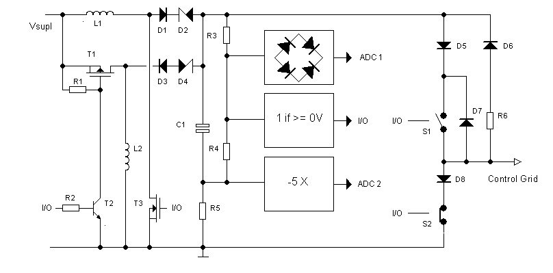
Figure 3.1 The circuit concept of the “bipolar” grid supply.
The concept of the circuit is shown in Fig. 3.1. Heart of the circuit is the bipolar electrolytic capacitor C1. Unlike normal electrolytic capacitors a bipolar type doesn’t have a polarity and can be charged to positive, as well as negative voltages. Since both the anode, as well as the cathode dielectrics in these capacitors have the same thickness, these bipolar capacitors have a much lower capacitance density as compared to normal capacitors. Usually these bipolar capacitors are only made for smaller capacitances and voltages, but Nichicon makes a very nice bipolar capacitor with a capacitance of 100 uF and a voltage rating of 100 V. To the left of C1 in Fig. 3.1 we find two boost converters, a normal positive step-up converter consisting of L1, T3, D1 and D2, and an inverting boost converter consisting of L2, T1, D3 and D4. Similarly to the boost converters in the uTracer 3 also these two boost converters are controlled by the micro-controller. The operation is very simple, when the micro-controller pulses the positive boost converter, positive charge packages are delivered into C1 making the capacitor voltage more positive. Pulsing the inverting boost converter delivers packages with negative charge to C1, making the capacitor voltage more negative. In such a way any positive or negative voltage limited by the maximum voltage rating of C1 can be set.
The purpose of zener diodes D2 and D4 needs some explanation. Normally when the output voltage of the positive boost converter would become lower than the supply voltage, blocking diode D1 would open preventing the output voltage from becoming lower than the supply voltage. Similarly, in the inverting boost converter blocking diode D3 would open for any positive output voltage preventing the output from becoming positive. By inserting a zener diode with a blocking voltage larger than the maximum output voltage this never happens, and can this circuit configuration be used to generate both positive as well as negative voltages. This obviously implies that the boost converters now first have to overcome the standoff voltage of the zener diodes before they can charge or discharge C1. Would this be a real power converter circuit it would have been a deadly sin to throw away so much power, however in this case the boost converters have margin enough, and a high efficiency is not relevant at all.
The way the voltage and the current are measured is only outlined in Fig. 3.1 in a schematic way. Negative grid biases do not cause a grid current so they don’t need to be measured. Positive grid biases will result in a grid current which causes a negative voltage drop over current sense resistor R5. We would like to have this voltage drop small compared to maximum output voltage range so say 1 V max. This means that a -5x amplification is required to connect to the ADC in the PIC. Perhaps by using a low off-set Op Amp like the OPA277 even a smaller voltage drop can be used. Measuring the output voltage is a bit trickier since it can be positive as well as negative. There are a number of ways to measure positive and negative voltages. I have chosen to use a precision full-wave rectifier to negate the negative voltages in combination with a simple comparator which gives the sign of the voltage.
The output stage is split into two parts. Negative bias voltages are directly applied to the grid via D6. Positive grid biases need to be pulsed since they might cause excessive grid dissipation. Here I imagine a similar switch circuit as used in the anode and screen supplies of the uTracer. D5 and D7 isolate the switch when the grid output is negative. The GIU obviously has to take the voltage drops in the current sense resistor and the output section into account in setting the capacitor voltage.
Bread board testing of the double-boost converter concept
The Easter weekend 2015 was an ideal moment to test the double-boost converter concept to see how it would hold in real life! A simple circuit was designed that pulses the positive boost converter until the maximum voltage (ca. 100V) is reached. Next the inverting boost converter is pulsed until the maximum negative voltage (ca. -100V) is reached after which the whole cycle repeats.
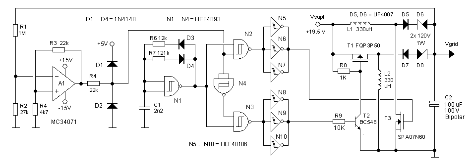
Figure 3.2 Bipolar grid-supply test circuit.
With the aid of two simple HEF CMOS logic building bricks the whole test circuit was realized without the need for a micro-controller. Heart of the circuit is the oscillator circuit around N1. This circuit produces an asymmetrical square wave with a pulse width of 20 us and a repetition frequency of 10 kHz, imitating the pulses produced by the PIC. These pulses are buffered by the HEF40106 inverters and used to drive either the positive boost converter or the inverting boost converter depending on the polarity of the output signal of Op-Amp A1. Op-Amp A1 is used as a Schmitt trigger which switches over at voltages below -2.5 or above 2.5 V (depending on R3 and R4). The output voltage of the boost converters is divided by R1 and R2 so that when the output is approximately 100 V (-100 V) the negative input of A1 is 2.5 V (-2.5 V). When the output voltage of the boost converters exceeds 2.5 V, the output of the Op-Amp becomes negative. The pulses are now directed by N3, N8, N9, N10 to the inverting boost converter so that the output voltage will decrease. When the output voltage drops below -2.5 V the positive boost converter is switched on and the cycle repeats.
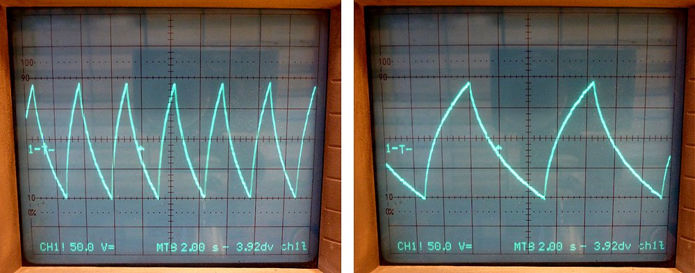
Figure 3.3 Output of the bipolar grid-supply test circuit, using a 20 us boost converter pulse (left), and a 10 us pulse (right).
The whole circuit works like a dream! Fig. 3.3 left shows a trace on my memory scope of the output voltage. The output voltage swings between -100 V and 100 V and back in approximately 3 sec. The positive boost converter seems slightly more efficient than the inverting boost converter. The boost converter firmware uses two pulse length. The standard 20 us for fast charging, and a 8-10 us pulse for slow charging that is used to accurately set the output voltage. The 10 us pulse is simulated by adding a second 12k resistor in parallel to R6. Fig. 3.3 right shows the charge-discharge cycle for the 10 us pulse length. In this case the complete cycle takes about 8 seconds.
Figure 3.4 Drain voltage of T1 (Fig. 3.2) with zoom in on the actual pulse (right).
The PMOS MOSFET FQP3P50 became quite warm during operation of the test circuit. This is due to losses in the MOSFET. The FQP3P50 has an on-resistance of 4.9 Ohm. During a boost pulse the peak current in the inductor rises to V*t/L = (20*20 us)/330 uH = 1.2 A. This causes a maximum voltage drop of approximately 5 V. Figure 3.4 shows the drain voltage of T2. The voltage drop over the MOSFET is clearly visible; note how during the boost pulse (a) the voltage decreases from 20 V to 15 V (right photo). Note also the deeply negative “discharge” pulse (b) after the boost converter pulse (left photo). It is this pulse which opens the zener diode and discharges C2. After the inductor has dumped its “charge” into the storage capacitor, the current through the inductor has become zero, however, the voltage is at that moment still the output voltage plus the zener voltage! This energy is now stored in all the capacitances of the circuit, e.g. the drain-source capacitance of the MOSFET. This energy has no way to go: the transistor is off and the diode is not conducting. As a result the energy will oscillate between the inductor and the capacitances in the circuit until it is dissipated by Ohmic losses in the circuit (c). Back to the voltage drop over the MOSFET during the boost converter pulse, the voltage drop can be reduced by selecting a MOSFET with a lower on resistance. That is not so easy. There are plenty affordable transistors with a breakdown voltage of -200 V and an on resistance of approximately 1 ohm (IRFR9220, IRF9630 or FQD5P20), but unfortunately -200 V is a bit on the low side. A compromise is the IRFR9214PBF with an on resistance of 3 ohm and a breakdown voltage of -250 V. At any rate the problem will not be all together that serious since the MOSFET will be driven with 10 us pulses most of the time anyway.
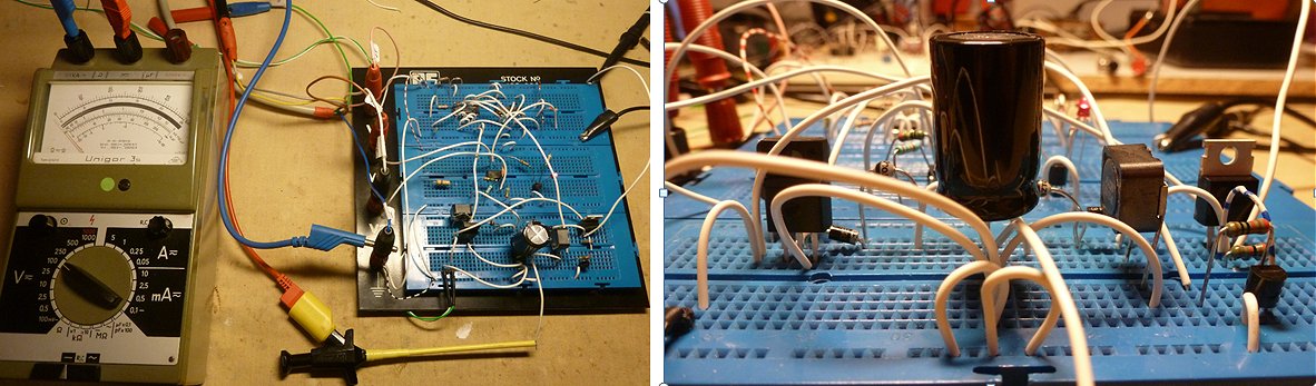
Figure 3.5 Easter 2015, the bipolar grid supply test circuit on breadboard.
Firmware implementation
Next thing is how to deal with this idea in the firmware. First thing is to sort out a way to represent the grid voltage in a convenient way. Using the circuit concept of Fig. 3.1 the reading from the ADC will be symmetrical around zero volts, and there will be an additional bit to indicate the polarity. The great advantage of this scheme is that there is no need for a (manual) zero calibration while still the unipolar ADC on the PIC can be used. The trick is to convert the data to a number that is compatible with the boost converter control routines. The best method seems to be to convert the 10 bit ADC data and the 1 bit sign information into an 11 bit number where 000 0000 0000 represent – 100 V, 100 0000 000 represents 0 V, and 111 1111 1111 is mapped to 100 V (Fig. 3.6 left). Note that here only the most significant byte is shown.
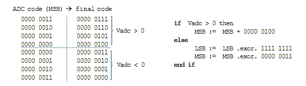
Figure 3.6 Converting the ADC output and sign bit into a useful representation.
Fig. 3.6 (right) also shows a simple algorithm to convert the measured data into the desired format. When the voltage is positive, only 0000 0100 is added to the most significant byte of the ADC output and the least significant byte is left untouched. When the voltage is negative the ADC output is inverted. Inverting a bit in assembler can be done by performing a Boolean .EXOR. operation with 1. Note that performing an .EXOR. operation with 0 leaves the bit unchanged. So to invert the lower byte an .EXOR. operation with 1111 1111 is performed while the lower two bits in the most significant byte are inverted by doing and .EXOR. operation with 0000 0011.
 The next step is to fit the bipolar grid supply idea in the existing boost converter control firmware (weblog 1,
weblog 2). The basic algorithm is very simple: when the output voltage is lower than the set point then pulse the positive boost converter, and when the output voltage is higher than the set point the inverting boost converter is pulsed! In this way the output voltage will stabilize itself around the set point. Since two pulse outputs are needed, they need to be controlled by two “mask bits”. The algoritm can now simply be implemented in the boost converter control routine: when Vout < Vset, set the mask bit for the positive boost converter; and when Vout > Vset, set the mask bit for the inverting boost converter.
The next step is to fit the bipolar grid supply idea in the existing boost converter control firmware (weblog 1,
weblog 2). The basic algorithm is very simple: when the output voltage is lower than the set point then pulse the positive boost converter, and when the output voltage is higher than the set point the inverting boost converter is pulsed! In this way the output voltage will stabilize itself around the set point. Since two pulse outputs are needed, they need to be controlled by two “mask bits”. The algoritm can now simply be implemented in the boost converter control routine: when Vout < Vset, set the mask bit for the positive boost converter; and when Vout > Vset, set the mask bit for the inverting boost converter.
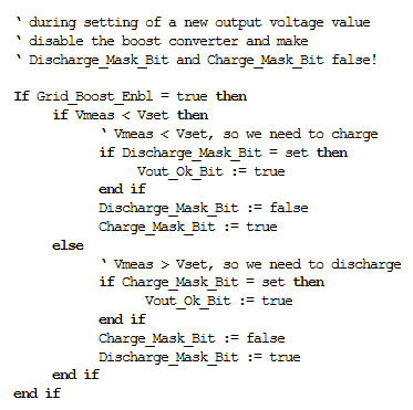
A little bit trickier was to find a way to decide whether the desired set point value has been reached. The method that I will probably implement is to look at a change in charging polarity: if in the previous cycle the positive boost converter was pulsed while in the present cycle the inverting boost converter is pulsed it means that the set point has been crossed and vice versa. The fragment of pseudo code to the left illustrates how such an algorithm can be implemented. It assumed that at the moment when a new set point value is loaded, the boost converter is disabled and that both the charge and discharge mask-bits have been cleared. The routine samples the data and establishes if the measured voltage is higher or lower than the set point. If, e.g. it is higher, the discharge mask-bit will need to be set, but the routine first checks if the charge mask-bit was already set. If so, the output ok flag is set, followed by an update of the mask-bits. All pretty straightforward and transparent
The full-wave rectifier
I was always under the assumption that full wave rectifiers were quite complex 3 or 4 OpAmp circuits, so I was pleasantly surprised to find a simple two OpAmp circuit well described in an
application note from Texas Instruments. The circuit was tested on breadboard to get some feeling for its behavior and to measure the offset with different OpAmps.
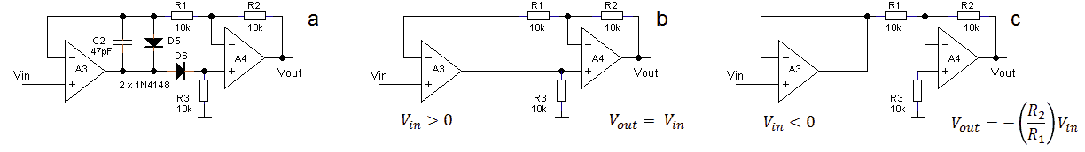
Figure 3.7 The full-wave rectifier circuit.
The full-wave rectifier circuit used in the tests is shown in Fig. 3.7a. The working of the circuit is quite simple. Assume that the input voltage is positive and that the output is initially zero (Fig. 3.7b). Diode D5 will now block while D6 conducts. The input of A4 does not draw any current, so the voltage on the inverting input of A3 will be equal to the output voltage of A4. The feedback loop will now adjust so that the output of A4 equals the non-inverting input of A3. Next assume that the input voltage is negative and the output initially zero (Fig. 3.7c). In this situation D5 will conduct while D6 will block. A3 now simply reduces to a buffer stage while A4 is switched as am inverting amplifier with gain A = -(R2/R1). So R2 and R1 need to be precision resistors with equal value.
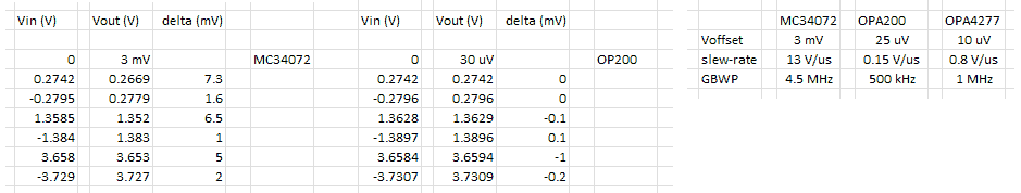
Figure 3.8 Full-wave rectifier test results.
As a concluding remark I would liketo add that this is just an idea. In its present form it cannot be added to the uTracer 3 mainly because in the uTracer 3 the cathode is not referenced to ground. Maybe it is a nice concept for a future uTracer version …?

Just a souvenir for myself of a beautiful stay in Lisbon May 2015. A panoramic view from Jardim de Săo Pedro de Alcântara - Jardim António Nobre.
| to top of page | back to the uTracer homepage |
If there is one aspect of the uTracer 3 that raised a lot of discussion, it must be the heater supply. Originally the heater supply was just meant as a nice bonus. There was a PWM output on the PIC left and with a simple driver and a power MOSFET a simple heater supply could be implemented. However, when people started to use the heater supply for more serious low voltage / high current heaters, this simple scheme turned out to be inadequate. The very short PWM pulses in combination with inductances in the wiring reduced the effective heater power considerably. Experimenting with a real Buck Converter had been for a long time on my list of things to do when a friend at TI recommended me the TPS54336.
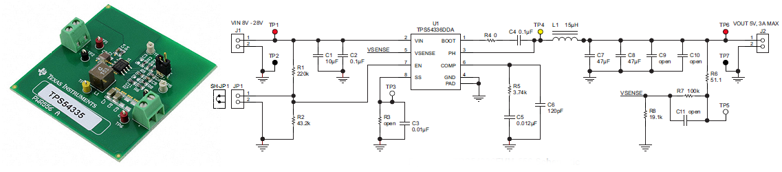
Figure 4.1 The TPS54336EVM-556 evaluation board and circuit diagram
The TPS54336 is a remarkable small step-down converter for that can deliver output voltages down to 0.8V at a continuous current of 3A. The inout voltage can be up to 28 V so that it can be directly fed from a 19.5 V laptop power supply. It comes with a whole load of useful features such an enable input, over current protection, high temperature shutdown etc. The only drawback for the amateur is that it comes in a small SO8 SMD package with a difficult to solder thermal pad.
The TPS54336 comes with a very nice evaluation board which makes it very easy to get started. The output voltage of the converter is set by two resistors (R7 and R8 in Fig. 4.1) that divide the output voltage down to 0.8 V, the reference voltage used in the output voltage control loop. The proper resistor values as a function of output voltage, or alternatively, the output voltage for given resistor values can be easily calculated using the equations in Fig. 4.3. The first thing I was curious to try was how the TPS54336 would perform driving an heavy EL34 heater, which has a cold resistance significantly lower than the resistance at the operating point. The evaluation board is factory set to 5 V (Fig. 4.1). By shunting R8 with a XXX resistor the output voltage was increased to 6.3V. Figure 4.2 shows the heater voltage during cold switch-on of an EL34. Within 5 ms the output voltage reached the set point value of 6.3 V! Even better, the IC remained absolutely cold. Even when driving a 2.2 Ohm power resistor (2.9 A @ 6.3 V), the IC didn’t show any significant temperature increase.
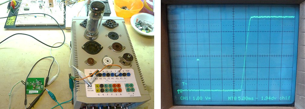
Figure 4.2 Right, first tests with the TPS54336 evaluation board. Left, switch-on behavior with a cold EL34 heater as load.
An adjustable step-down converter with the TPS54336
By replacing the fixed resistor R8 in Fig. 4.1 with a digital potentiometer, it is possible to make the output voltage adjustable by the micro-controller. For this I selected a potentiometer from the MCP41XXX series from Microchip. These potentiometers are cheap, readily available in both SMD and though-hole packages, and have a simple SPI interface. These potentiometer chips come in three resistance values: 10k, 50k and 100k.
As it happens this plan is less straight forward than it seems at first sight. The problem is related to the fact that the reference voltage is quite low, and secondly that we want to cover quite a large voltage range from say 1.5 to 12V. The output voltage is roughly proportional to R1/R2, so in order to set the output voltage to say 12 V, the ratio of R1/R2 (Fig. 4.3) becomes quite large: 14. This in turn means that R2 has to become quite low, and we enter a region where the output voltage change as a result of a resistance change becomes quite large (dVout/dR2 is high). Now unfortunately the digital potentiometer only has a resolution of 8 bits so that the minimum resistance step is limited to Rtot/256. This means that, whereas the resolution for low voltages is very fine, it becomes coarser at higher voltages. To get an idea: with R1 = 30k, and R2 a 50k potentiometer, the values around 12V are: n=9 Vout=13.5V; n=10 Vout=12.3; n=11 Vout=11.32. So in this simple scheme it is simply impossible to set the heater voltage exactly to 12V. Since 12 V heaters are very common I can imagine that most people would find the error at especially unacceptable.
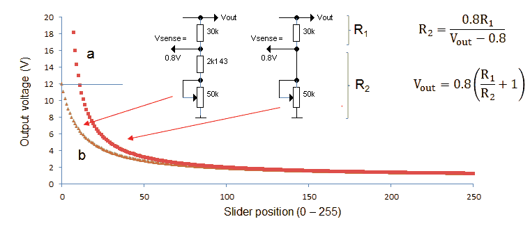
Figure 4.3 Output voltage as a function of wiper position.
To make things even worse, digital potentiometers are not ideal components in the sense that the tolerance in the total potentiometer resistance can be quite high (a nom. 50k potentiometer can vary between 35k and 65k), and that they have a parasitic wiper resistance, which for the same potentiometer is typically 125 ohm but can be up to 175 ohm. It is clear that it is impossible to get an accurate 12 V output set-point only using a software calibration procedure. The solution that I implemented is therefore based on the following assumptions:
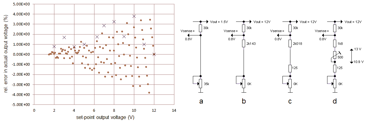
Figure 4.4 left, calculated relative error in the output voltage as a result of the finite resolution of the digital potentiometer. Right, the design strategy step-by-step.
The following design strategy was used:
At this point we can calculate what the error for any given voltage will be in the final circuit. For every slider position the output voltage was calculated and stored in an array. Next the full output voltage range from 2 to 12 V was scanned in increments of 0.1 V and for every voltage the closest output voltage value in the array was determined. From that value the relative error was calculated and plotted (Fig. 4.4 Left). Note that the 12 V set point value is perfect (because we made it to be so) and that furthermore the maximum error is about 2.5% which quickly drops for lower output voltages.
A Test Board
To test the TPS54336 in combination with the digital potentiometer MCP41050 and a PIC controller a special test board was made. Heart of the test board is the TPS54336 evaluation board.
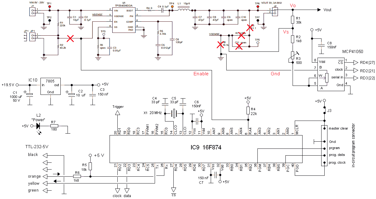
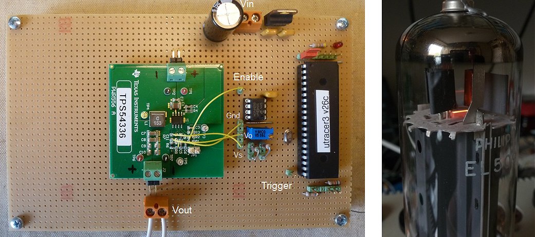
Figure 4.5 Circuit diagram of the buck converter heater supply based on the TPS54336 (top) and the implementation on perf-board (bottom).
Lighting up the 6.3V/2A heater of an EL509 is a piece of cake for the tiny circuit!
Figure 5 shows the circuit diagram of the test board. The circuit is pretty straightforward and is based on the uTracer 3 hard- and firmware. The digital potentiometer interfaces with the SPI control lines already used for the PGA’s. A new SPI firmware routine was written which first send the command byte 011H to the potentiometer to indicate that the commend is a new setting and that potentiometer one is addressed (there is only one potentiometer), and next sends the wiper position byte which is the lowest byte of the heater setting send by the GUI. Value 000H (wiper to B) corresponds to the highest voltage (12 V), and value 0FFH (wiper to A) corresponds to the lowest voltage. The open drain output RA4 is used to control the enable pin. Although the enable input of the TPS54336 has a pull-up current source of 1 uA, I added an additional pull-up resistor of 22k to improve noise immunity. The firmware has been adapted so that when a ping command is given, the TPS54336 is disabled for approximately 1 ms to study the enabling / disabling behavior. A trigger signal to capture the event is available on pin 20 of the PIC.
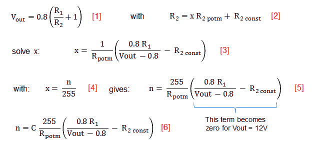
Figure 4.6 These equations relate the potmeter setting to the desired output voltage.
The equations in Fig. 4.6 explain how in the GUI the heater voltage setting (Vout) is converted into an 8 bit setting for the digital potentiometer. Starting point is equation [1] which gives the output voltage of the TPS54336 as a function of the value of the “top” resistor R1 (see also Fig. 4.3) and of the “bottom” resistor R2. R2 consists of a variable part (the digital potentiometer) and a constant part (the trimmer, the fixed resistor and the slider resistance). The variable part can vary between zero (x=0) and the maximum potentiometer resistance R2potm (x=1). Substituting [2] in [1] results in an equation which gives x as a function of the desired output voltage [3]. The variable x depends on the setting of the digital potentiometer according to [4], with n any value between 0 and 255. This finally yields n as a function of the output voltage [5].
The second term in Eqn. 5 is constructed in such a way that the term becomes zero for 12V. So the value programmed in the GUI for R2const exactly equals 0.8*R1/(Vout-0.8). So with R1 = 30 k the value of R2const = 2.143k (see also Fig. 4.4b). Note that this corresponds to adjusting the output voltage to 12V for n = 0 with trimmer R3. Finally, we have to account for the tolerance in the value of the digital potentiometer. This can be simple done by adding a constant C [6] which is determined using a second calibration point. In summary the calibration procedure is now as follows:
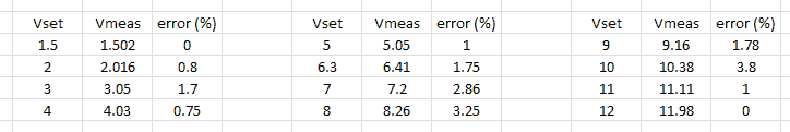
Figure 4.7 Measured output voltage as a result of a set point entered in the GUI. The load was in all cases a 12V / 20W halogen light bulb.
Figure 4.7 gives, following the calibration procedure described above, the measured output voltage as a function of a certain set point. As expected the error in the output voltage increases with increasing voltage but is limited to a few percent. The errors have also been plotted in Fig. 4.4 and remain within the error range expected. The tiny circuit can easily drive loads of up to 3A without even getting notability warm!
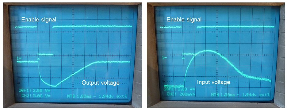
Figure 4.8 Enable signal (top trace in both photos) and on the lower trace the output voltage (left), and input voltage (right).
The output voltage was in both cases set to 12 V and the load was a 12V / 20W light bulb.
Concluding:
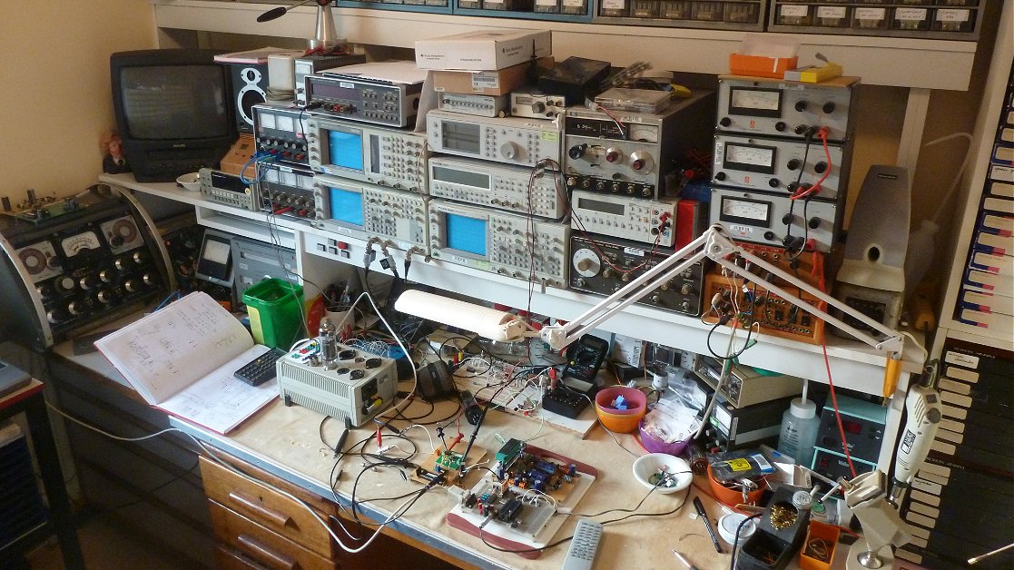
A photo for posterity. My “man cave” on the 5th of May 2015. In the center the buck converter test board. To the right my ISP PIC programmer and test uTracer (on this set all PICs sold have been programmed and tested). To the left an EL509 as a test load for the buck converter. Note on the extreme left my brand new fantastic AVO-IV that I got from a colleague as a present !!
| to top of page | back to the uTracer homepage |
The previous section generated, judging by the number of emails I received, a lot of interest among readers. Among the many suggestions and comments was a very interesting design idea by Tim Nightingale. Tim suggested a very simple idea to obtain a linearly programmable Buck converter that he had used in a design of himself.
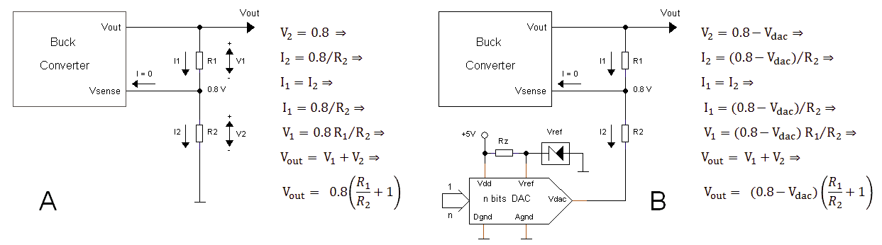
Figure 5.1 A) Standard buck converter, B) Linearly programmable Buck converter.
The easiest way to understand Tim’s idea is to first have a look at the feedback loop of normal Buck converter (Fig. 5.1A). It is important to realize that the Buck converter adjusts its output voltage so that the voltage on the Vsense input equals the reference voltage, in case of the TPS54336 0.8 V. The voltage on the node of R1 and R2 is thus always 0.8 V. The current through R2 is therefore given by 0.8/R2. Since the input current of the Vsense input is negligible, the current though R2 must therefore also pass through R1. The voltage drop over R1 is therefore R1*(0.8/R2). The output voltage is therefore 0.8 + R1*(0.8/R2), or 0.8*(R1/R2 +1).
Note that the output voltage varies linearly with the current through R2. In other words, if we can find a way to program the current through R2, we can program the output voltage. This is exactly what the idea of Tim does! Rather than connecting R2 to ground, it is now connected to the output of a DAC (Fig. 5.1B). When the output of the DAC is 0V, the current through R2 and thus the output voltage are maximal (same situation as Fig. 5.1A). When the output voltage of the DAC increases, the current though R2 - and thus the output voltage - decrease proportionally. This continues until the output voltage equals the reference voltage. Note that the output voltage swing of the DAC needs to be slightly less than 0.8 V.
Using a DAC higher reference voltage
Although the above idea sounds very attractive, it has a practical disadvantage and that is that the DAC should have an output range of 0 to 0.8 V. This implies either the use of a very low reference voltage e.g. 1.225 V (LM4041) and/or using only a fraction of the output range of the DAC which is a waste of bits!
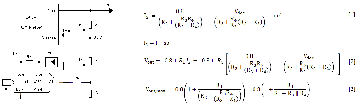
Figure 5.2 Using the circuit with higher DAC reference voltages
Figure 5.2 shows a more elegant circuit implementation. Instead of connecting R2 directly to the output of the DAC, it is connected to the center node of a resistive voltage divider consisting of R3 and R4. Without any calculation, just by reasoning, we can understand how the circuit works. To do this we use the super position theorem and the notion that the output voltage increases linearly with the current through R2 (previous subsection). Now consider the subcircuit formed by R2, R3 and R4. This circuit is being excited by two voltage sources namely the reference voltage (0.8V), and the output voltage of the DAC. To calculate the current through R2 we calculate the current as a result of the individual voltage sources while the other voltage source is set to zero (short circuit), and then we sum the results. The left term in Eqn. 1 (Fig. 5.2) is the current through R2 as a result of the reference voltage while the DAC output is 0 V. The second term in Eqn. 1 is the current through R2 as a result of the DAC when the reference voltage is set to 0 V. Note that this component of the current is negative! So when the DAC output is 0 V, the current will be highest and the output voltage will be maximal. When the output voltage of the DAC increases, the current will decrease linearly with the increasing DAC output voltage. This will continue until the output voltage equals the reference voltage. Equation 2 gives the exact output voltage, while Eqn. 3 gives the maximum output voltage for given R1, R2, R3 and R4.
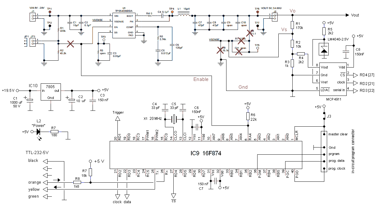
Figure 5.3 The test circuit
To test the whole idea, the test board made for the “potmeter buck converter” in the last section was extended with a DAC and a reference voltage source. For the DAC I choose an MCP4911 from Microchip. This DAC is cheap, comes in an 8 pin DIL package and has a digital SPI interface. For the voltage source I used a 2.5 V version of the LM4040 in an TO-92 package from TI. Figure 5.3 shows the circuit diagram of the test circuit.
Although it is possible to express R1 … R4 directly as a function of a set boundary conditions, I choose the easy way and made a small program that gives the output voltage as a function of R1 … R4 for the minimum and maximum DAC output voltage, and I determined R1 … R4 directly by “trial and error” which turned out to be quite easy.
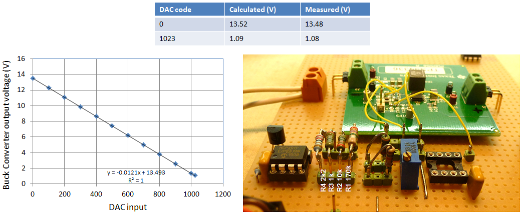
Figure 5.4 Measurement results and DAC circuit close-up.
The table in Fig. 5.4 shows the calculated and measured output voltages for the minimum and maximum output voltage of the DAC. It is surprising that, although just standard resistors were used and nothing was calibrated, the measured output voltage matched the calculated within a percent or so! The graph shows the extremely linear variation of the output voltage with the programmed DAC value. In fact when a straight line was fitted through the data points the R-squared was exactly one, indicating a perfect fit!
Loose Ends
| to top of page | back to the uTracer homepage |
A Bluetooth interface for the uTracer
There are two ways of installing a Bluetooth interface to the uTracer:
1 – A HC06 module directly connected to the Tx and Rx of the uTracer PIC
The HC06 is a serial Bluetooth interface module which is very popular in the Arduino world; you can buy these devices for as little as €3 to €5 on eBay. It is based on the CSR BC417 BT chip (Cambridge Silicon Radio Limited).
The advantage of the HC06 is that the default settings correspond to the uTracer communication parameters: Baud rate: 9600N81. This makes the module almost “plug and play” for our application. The ID is: “HC-06” and pairing password is “1234”. All parameters can be altered with the “AT” configuration commands of the HC06 but we don’t need it for our purpose (see datasheet for details, If you like you can change the name from HC-06 into “uTracer” or alter the pairing code.)
Click here
Click here for more info on these modules.
This HC06 module comes on the ZS-040 backplane which has some interfacing circuitry and a low drop regulator to provide 3.3 V. It has also a red (SMD) LED to indicate the BT pairing status
(Click Here for an Ebay link).
(Be sure to get a HC06 on a ZS-040 backplane, these are tested – other backplanes are not tested)
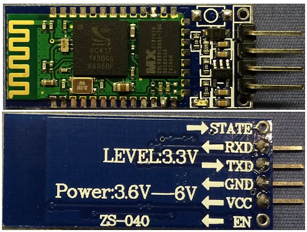
Figure 6.1 The ZS-040 HC6 bluetooth module.
The ZS-040 HC06 module communicates via a 3.3 V serial connection. It has four pins:
2 – Interfacing the HC06 module via the RS232 connector.
The popular HC06 module is also available mounted on another backplane with a MAX 3232 IC on board and equipped with a male and a female DB9 connector. This version (BT<->RS232 V1.3 JY MCU) makes life even a lot easier, the male DB9 connector (DTE) can be plugged directly in the female DB9 RS232 connector of the uTracer. On board is a 3v3 regulator and the V+ is protected against reverse polarization by a Schottky diode in series. The female DB9 (DCE) can be plugged on the computer RS232 to change parameters like the name of the module or pairing code, standard “HC06” and pairing code “1234”. You need a terminal program for this. But this step is optional, the module’s default settings match to the uTracer communication parameters: Baud rate: 9600N81.
The only modification we have to do is providing 5 V to the module. This can be done easily: solder a wire from pin 9 of the male DB9 connector to the V+. On the uTracer side you do the same by soldering a wire from pin 9 of the female DB9 to 5V on the uTracer. Pin 9 of a standard RS232 connector is the RI (ring indicator) input of the RS232 and is normally not used anymore and putting 5V on pin 9 should do no harm to a connected computer or USB RS232 converter. The original function of the RI was for modem connections – The signal was -3V to -12V when idle, and +3 to +12V when the telephone was ringing.
Figure 6.3 The HC06-RS232 Bluetooth module with RS232 port
This HC06-RS232 (Arduino DB9 RS232 RF Wireless Bluetooth Module HC-06 Slave Serial Port) costs around €8 on eBay (Click here for an Ebay link).
Instead of a plug-on module you can build the BT<->RS232 into your uTracer cabinet and select between standard RS232 and Bluetooth connection with a switch.
An alternative BT solution is to buy a “Plug-and-play” Bluetooth Serial Adapter in a nice housing.
Mouser sells The “FireFly Bluetooth 2.0 Serial Adapter” series. Choose the RN-240M, this has a male DB9 connector. This adapter is also powered on pin 9 of the RS232 connector. Click here for a link to the Mouser page.
The uTracer Quick Test Android App
With this App you can do a Quick test just like the Quick Test in the GUI:
The only difference between the GUI and the App is that the delta used for the tube parameters is fixed to 10%. If the selected Anode and screen voltage is too high (which would cause a voltage higher than the maximum – 300V or 400V depending on the uTracer version), then only the Anode and Screen currents are measured.
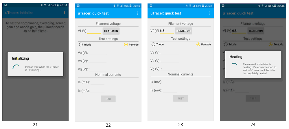
Installation Steps:
(see screenshots for an installation on an Android phone – in this case a Samsung Galaxy J5)
Preparation:
The Bluetooth interface of the uTracer must be active (Blinking Led on the module).
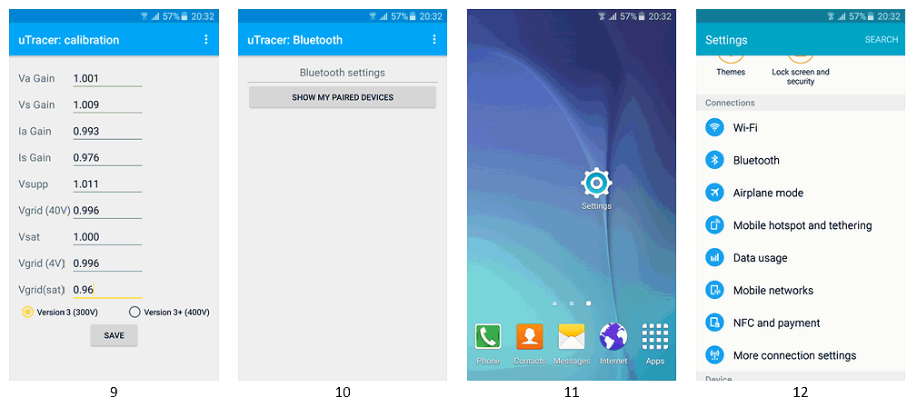
Make sure you have the calibration values for your uTracer at hand (take a screenshot of the calibration menu of the GUI or write them down).
1)
Install the Quick Test App from the Google Play Store:
https://play.google.com/store/apps/details?id=be.michielvk.utracer3
See pictures of screen shots.
It can be installed on Android phones and tablets running Android 4.1 and higher.
(You have to the steps below only once to prepare your phone or tablet for the uTracer App)
2)
The App asks your permission for Bluetooth access.
Select “Accept”.
3)
The App is now downloading and being installed on your Android device.
4)
After successful installation the App opens with a welcome screen.
“Welcome to the uTracer app!”
“Tap the arrow to get started!”

5), 6) ,7)
The three following screens give some info on how to access the Calibration and Help menu.
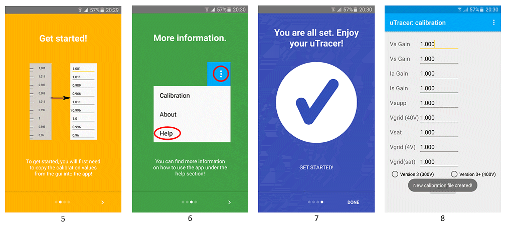
8), 9)
Next the calibration screen is opened and a new default calibration file is created.
Enter all GUI calibration values from your uTracer.
Also very important: select between uTracer3 or 3+ for the uTracer version you have.
Tap “SAVE”.
10)
Next screen shows: “SHOW MY PAIRED DEVICES”.
11)
Now go to your Android Home screen and look for your “Settings” icon (this can look different depending on your Android version and/or the brand of your device).
Tap on “Settings”.
12)
Select: “Bluetooth”.
13), 14)
Turn on Bluetooth to see a list of available BT devices and their pairing status.
15)
In “Available devices” select: “HC-06” (in case your BT module is a HC-06).
16)
Depending of your Android device you need to repeat this a few times until a “Bluetooth pairing request” appears.
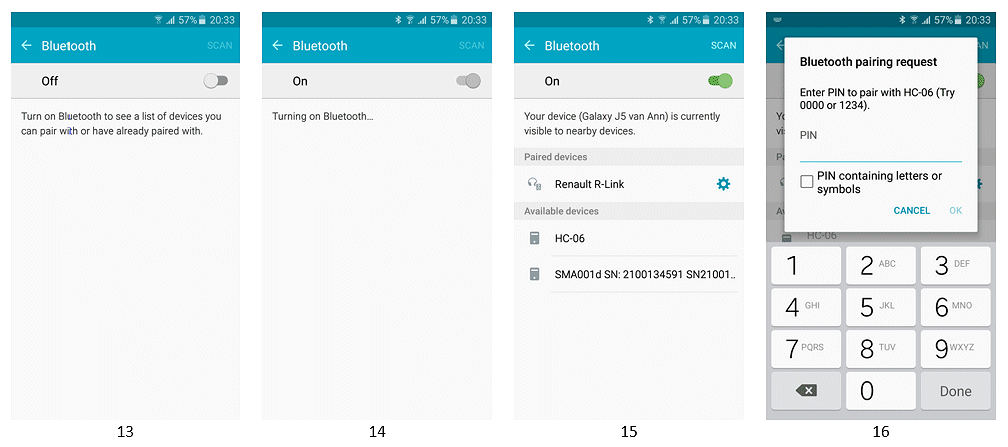
17)
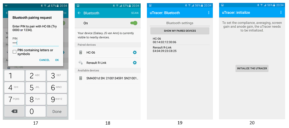
Now enter the pairing code (default “1234” for the HC-06) and tap “OK”.
18)
In next screen you’ll find the HC-06 in the list of paired devices.
Now, your phone or tablet is paired with the BT module and will also do so in future.
After this installation, next startups of the App will show the screens described under Step 19. You will not see any more the installation screens. You can always access the help- and calibration screen by taping on the three Android dots in the upper right corner.
Do a Measurement
19)
In the App you’ll see the HC-06 (with its native MAC address) listed under “SHOW MY PAIRED DEVICES”.
Select the HC-06.
Now your phone or tablet makes connection to the HC-06 module and the Blinking Led on the module changes to a steady “On”.
20)
You come to the “initialization” screen.
Tap “INITIALIZE THE UTRACER”.
Note: in the next version the “Initializing” will be done automatically after 19)
21)
The window “Initializing” pops up for some seconds.
22)
Now you can start a measurement (connect the “Tube under Test”).
23)
Enter the filament voltage and tap “HEATER ON”.
24)
The window “Heating” pops up for 20 seconds and the tube starts heating.
Remark: You always have to enter the Vf and tap “HEATER ON” even if you are using an external heater power supply.
25)
Select between “Triode” or “Pentode”.
Enter the test parameters and tap “Test”.
26)
In this case a double triode ECC40 will be tested.
We select Triode and we enter set point values for Va1, Va2, Vg and the expected nominal anode currents, for an ECC40 this is 6 mA.
Tap “Test”
The “Testing” window pops up for about 10 to 20 seconds.
Remark: in case you test a single triode: don’t enter 0 V for Va2, this causes an error (uTracer fails to return a character in a reasonable time). Enter at least 5 V or enter the same value of Va1. In the next version the minimal value of Va will be automatically increased to 5 V when entering a lower value.
27)
The “Results” window appears.
In this case (Triode) the measured values for Va1,Va2, Ia1,Ia2 are displayed and the percentage of the Ia versus the nominal Ia currents for this tube.
Because the set points + 10% are all lower than 300V a full measurement is done and the Ra, gm and mu are calculated and displayed. (limit of 300V for uTracer 3 in this case – for an uTracer3+ the limit is 400V).
To obtain a full measurement the -Vg also needs to be higher than 0 V, when entering Vg=0V only the anode currents and the percentages of their nominal values are measured.
Remark: Just like with the quick test in the GUI you may play a bit with the applied Va- value to obtain a more exact test value of Va, in this case a 252V set point results in measured test values of 250.1 V and 250.9V.
28)
When taping on “OK” you return to the previous screen where you can alter test parameters and re-test or you can Abort: the heating stops.
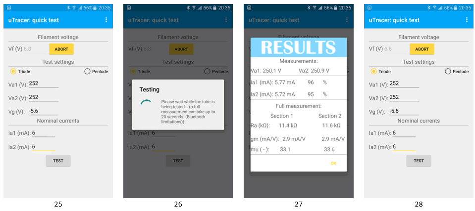
29)
Closing the App.
It is important to abort before closing the app otherwise the heating will stay on while the phone or tablet is disconnected from the uTracer.
When you hit the Android back button the app asks if you are sure you want to exit.
Tap “Yes” and the app closes.

| to top of page | back to the uTracer homepage |
A few months ago, I stumbled upon the beautiful web page on low voltage tubes by Jeff Duntemann. It very nicely re-introduced me into the world of low-voltage tube electronics.
I knew it existed, in the past I have collected nice set of low-voltage car radio tubes (ECC86, ECH86), and a small box full of hearing aid tubes, but to be honest I didn’t give the topic much attention so far. What fascinated me was that also normal tubes can be quite effective at very low anode voltages, be it that they cannot generate substantial amounts of power.
 Nevertheless, people have successfully constructed radios and headphone amplifiers operating at voltages as low as 12V. In the past already a number of people have asked me questions about the performance of the uTracer at very low voltages (0 – 20V). Unfortunately that is not very good. The simple design of the uTracer was optimized for a large operating range at the expense of performance at the very low voltage range. Because I wanted to experiment with low voltage tubes myself now after Jeff Duntemann had raised my interest, I decided to spend the 2016 Christmas Holiday by modifying the uTracer for low voltage / low current operation. The target specification that I set for the “uTracer3LV” were:
Hardware and software modifications
To facilitate the experiments, a special test version of the uTracer was built. To make an easy changing of crucial components possible, modified pin headers where inserted in between the PCB and some components. To start with, the standard uTracer3+ configuration was built as a reference. Instead of using tubes during the initial tests, I prefer to use a resistor as test devices because they give a much clearer indication of the quality of the measurement, and apart from that they don’t require heating up.
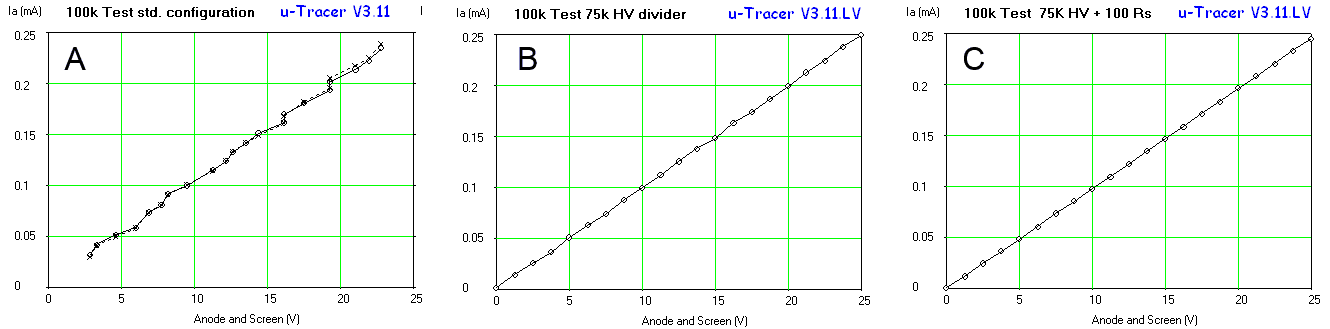
Figure 7.1 100k test resistor results for: A. standard uTracer3+ configuration, B. same with high voltage divider resistor lowered to 75k, C. same with current sense resistor increased to 100 ohm.
Figure 7.1A shows a measurement of a 100k resistor in the standard uTracer3+ configuration. The first thing we notice is that the curve looks rather ragged. The second annoying shortcoming is that the curves don’t extend all the way down to 0 V. There are potentially two causes for the ragged look of the curves. In the first place the relative accuracy of the AD converters that control the anode and the screen voltages is rather low in this bias regime. For the 10 bits AD converters, every LSB represents a voltage increment of approximately 450/1024 = 0.45 V. While that is fine for an anode voltage of say 200V, it is not enough for these low voltages. The other reason for the ragged look is related to the discrete amounts of charge that are injected into the reservoir capacitor in a single cycle of the boost converter. We will deal with this issue later but first look at the AD converter.
The obvious first thing to do is to modify the circuit in such a way that a smaller anode voltage range is mapped to the full range of the AD converter. By simply decreasing the value of the 470k resistor in the high voltage divider to 75k, the voltage range is decreased to 76V (50V operating range + 25V supply voltage). This increases the resolution of the AD converters to less than 0.1 V. Obviously the GUI also has to modified for the correct conversion factor. Figure 7.1B shows that this simple measure alone already greatly improves the linearity of the measurement. Figure 7.2 shows the standard anode supply circuit and the final low voltage circuit on the right with all the modifications for low voltage operation highlighted. In the remainder of this section we will go through the other modifications one by one.
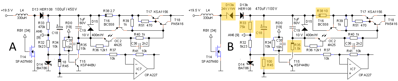
Figure 7.2 Anode high-voltage supply of the original uTracer3+ (left), and the same circuit adapted for low voltages and low currents (right).
The Screen section is identical to the anode section.
Unfortunately, things are not as simple as that. After every voltage sweep, the discharge transistor T15 (and the corresponding transistor in the screen section) discharges the reservoir capacitor to prepare it for the next sweep. Discharging continues until the HV-led is off. In the firmware a very simple algorithm is used to check if the discharging of the reservoir capacitor is complete. In short, when the output of the ADC is 0000XXXXXX the capacitor is considered to be discharged. In the original circuit this corresponds to a voltage slightly higher than 22V. With the high voltage divider modified, this value is however mapped to 4.7 V. It will be remembered that in the standard boost converter circuit the reservoir voltage cannot be lower than the supply voltage (19.5 V). Since we wanted to include 0 V in the measurement range anyway, zener diode D13a was added. This zener diode blocks the supply voltage at the expense of efficiency. Since this is not an issue for this low voltage version, it is a simple and elegant solution to include 0V. But even now the reservoir capacitor voltage cannot be decreased below 10 V due to D15. The firmware was therefore modified so that discharging continues until the output of the ADC corresponds to 00XXXXXXXX, corresponding to 19 V which is nicely between the supply voltage (allowing for 0V output) and the 10 V of D15. Unfortunately however, this does require a modification of the PIC’s firmware. While we are at it, the discharge resistor R35 was lowered in value to 1.5k to match the lower voltages, and to enable faster discharging.
The hardware and software thus modified produced the curve in Fig. 7.1B, not a bad starting point! The curve was however produced with a 32X times averaging to reduce the noise in the current measurement. A simple alternative to reduce noise and extend the current range to lower values is to increase the value of the current sense resistor. The value of this resistors is determined by the maximum input voltage of the PGA (5 V) and the maximum current to be measured. Since for low-voltage tubes the currents rarely exceed several tens of milliamps, the maximum current was chosen to be 50 mA, resulting in a sense resistor of 5 / 0.05 = 100 ohm. Figure 7.1C shows for comparison exactly the same measurement as in Fig. 7.1B (32 X averaging) but now with the 100 ohm current sense resistor.
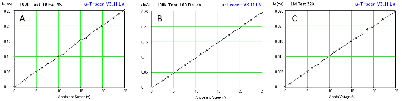
Figure 7.3 A and B: effect on noise of increasing the sense resistor to 100 ohm for a 100k test resistor with only 4X averaging. C: With the low voltage uTracer it is possible to measure anode and screen currents down to 1 µA.
In Fig. 7.3A and B, the 100k measurement is repeated but now with only 4X averaging. Note that with the 100 ohm sense resistor a significant reduction of noise is obtained allowing for faster measurements. In Fig. 7.3C a 1M test resistor was measured. Note that good measurements are possible down to 1 µA. To make this possible the automatic averaging algorithm was also modified a bit. The automatic averaging settings are now: gain 1, 2X / gain 2, 2X / gain 5, 4X / gain 10, 4X / gain 20, 8X / gain 50, 8X / gain 100, 16X / gain 200, 32X. For the lowest current setting range I would recommend using a manual setting of 32X. Changing the automatic gain settings again required some firmware modifications of the PIC.
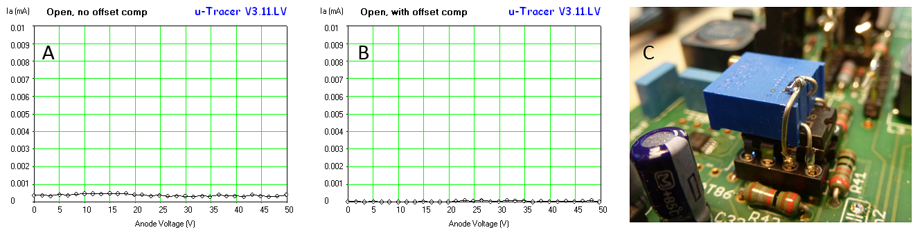
Figure 7.4 A – Measurement with open terminals. The offset in the anode (and screen) currents as a result of offset of the OPA227. B – Offset compensated open terminal measurement with a 20k potentiometer connected to the offset compensation pin (C).
With the output terminals of the uTracer open, a small offset of about 0.5 µA became visible. This offset is caused by the offset of the OPA227 OpAmps. For any practical purpose an offset that small is negligible, however just for the sake of fun, I tried to compensate it by using the external offset compensation pin of the OPA227. By “piggy backing” a small 20k 10-turn potentiometer on the back of an OPA227 it was possible to nicely tune away the offset, however it seems at the expense of a slightly increased noise level. It was fun trying it, but I think I won’t bother in the final setup.
Another simple tweak was the adjustment of the current compliance ranges and the hardware current limit. To start with the latter one, by increasing R38 from 2.7 ohm to 10 ohm the hardware current limit was decreased to approximately 65 mA. The software current compliance values cannot be chosen freely, but depend on the reference voltages that can be generated internally in the PIC (read more here). The following compliance ranges were implemented: 2 mA, 4 mA, 10 mA, 15 mA, 20 mA, 35 mA.
Figure 7.5 Output curves of an EF97 with 100 uF reservoir capacitors (A) and 470 uF caps (B).
The final tweak is related to the reservoir capacitor C18. It is the principle of the boost converter in the uTracer that this capacitor is charged to a certain value by packages of charge that are dumped into it by the inductor. Despite the fact that these packages of charge are relatively small, they nevertheless cause discrete increments in the voltage of the capacitor. The result is small variations in the anode and screen voltages, especially at lower voltages (read more here). This noise became apparent during the testing of a low-voltage EF97 pentode (Fig. 7.5). Observe that the “horizontal part” of the output characteristics is rather noisy (Fig. 7.5A). This was traced back to small variations in the screen voltage caused by the “charging packages.” Since the voltage increment for a given charge package can be decreased by increasing the capacitance, the simplest solution was to increase the value of C18, which is not that difficult since the operating voltage of the capacitor has decreased from 450 V to less than 100 V. Increasing C18 to 470 µF / 100 V, suppressed the noise effectively (Fig. 7.5B).
First measurements
ECC86 low-voltage double-triode
In the fifties a series of low-voltage radio tubes was developed for application in car radios. These tubes were designed to operate from 6.3 and 12 V power supplies. Although these tubes operate quite well as RF and IF frequencies, they cannot generate substantial power. In Europe – to my knowledge – only a few low-voltage car radio tubes were introduced with the ECC96, ECH86 and the EF97/EF98 as the best known examples. In the US many more tubes were developed (read more here). The 12K5 seems to be a very good example, but unfortunately I do not have that tube.
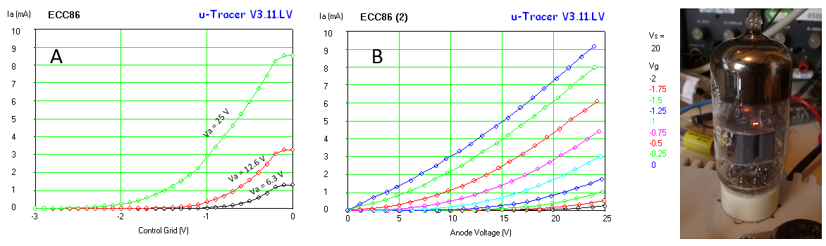
Figure 7.6 Ia(Vg) and Ia(Va) curves of the low-voltage double triode ECC86. Note the bright heater, indicating a high cathode temperature to increase emission.
The measured curves nicely match the curves in the datasheet. The leveling off of the Ia(Vg) curves at -0.1 – 0 V is because for these low grid biases, the grid starts to draw significant current and unfortunately the uTracer grid supply was not designed to supply current. However, the curves can easily be extrapolated to find the 0 V grid voltage anode current (more about grid current later). Note by the way how bright the filament in these tube is! One of the ways to obtain significant current at low voltages was to increase the emission by heating the cathode to higher temperatures.
Figure 7.7 Despite the fact that the anode currents of this ECC86 are somewhat lower than the values specified in the datasheet,
the transconductance and the amplification are still perfectly on spec.
DF64 hearing aid tube
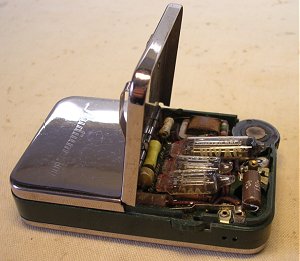 Already my whole life I have a fascination for hearing aid tubes. One of the reasons must be that already all my life we have “in the family” a hearing aid with three miniature tubes (see picture on the right). The hearing aid is operated from a 1.5 heater battery and a 22.5 V plate battery. I faintly remember that I have heard it working in my youth, but it has been silent ever after. In the meantime I have collected a nice set of hearing aid tubes found here and there, but never done anything useful with them. I even have a few sockets for these tubes and for the occasion I made an adaptor board to be able to test them in a comfortable way. The DF64 has a heater that is specified for 0.625 V at 10 mA. In this way two DF64 heaters can be switched in series and connected to a single 1.5 V cell. Since I do not like to drive the delicate heater from the PWM modulated heater supply of the uTracer, I included a holder for a 1.5V AA cell on the adapter board. A 100 ohm resistor reduces the heater voltage to approximately 0.625V.
The tiny pentode works better than expected from the datasheet. Whereas the datasheet specifies an anode current of 150 µA at Vg = 0V and Va = 15 V, the actual anode current is closer to 210 µA. What is also striking is that the curves in reality look a lot less pretty than the ideal curves in the manufacturer’s datasheet!
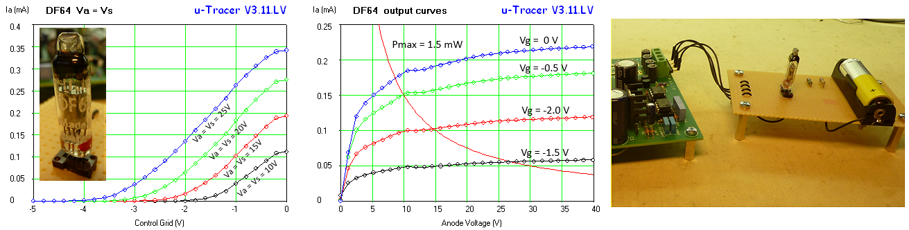
Figure 7.8 Ia(Vg) and Ia(Va) curves for a DF64 hearing aid tube.
DM160 indicator tube
The DM160 (CV6094) has been referred to as the first VFD display. It is a miniature indicator tube introduced by Philips in 1959. Its diameter is only 5 mm while its length is 2 cm. It was developed to be driven directly by digital transistor circuits without the need for a separate driving transistor. The DM160 consists of a filament and two grids. The second grid is coated with a fluorescent material so that it glows when it is hit by electrons (read more here). Somewhere I have read that people use this indicator to make amplifiers with it, so naturally I wanted to investigate the tube’s characteristics (Fig. 7.9). Personally I doubt whether the tube is useful as an amplifier, however, it is nice to study its characteristics at these low voltages.
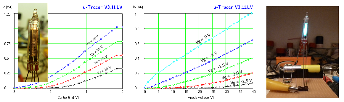
Figure 7.9 Ia(Vg) and Ia(Va) curves for a DM160 indicator tube
Several double triodes compared
Fig. 7.10 shows a set of Ia(Vg) curves to compare different double triodes with the ECC86. As Jeff Duntemann already concludes, the tubes with the highest anode currents at low voltages tend to be tubes that are specked for rather high heater currents and a relatively low maximum anode voltages like the ECC84 and the E188CC. Also the “special quality” E90CC designed for digital computers appears to be an interesting tube to experiment with.
Note again the deviation from the expected behavior for grid voltages around 0 V caused by the fact that for low grid biases tubes start to draw significant grid current, especially for low anode voltages.
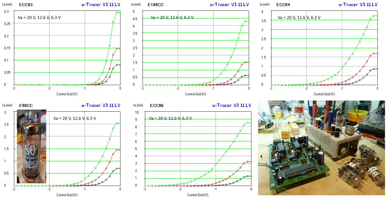
Figure 7.10 Ia(Vg) curves for several double-triode tubes.
Conclusion
With a few simple hardware and software modifications it is possible to make the uTracer suitable for the characterization of tubes at very low voltages. Unfortunately, this does require the modification of the PIC firmware. At very low anode voltages it appears that tubes start to draw significant grid currents for grid biases between -0.2 – 0 V. This grid current increases for lower anode voltages since less electrons are attracted by the positive anode. The present uTracer grid bias generator is not capable of sinking grid currents, resulting in an erroneous current reading in this grid bias regime, which is unfortunately of interest for low voltage applications. At the moment I am looking into a grid bias supply that can supply grid currents and even generate positive grid biases. The circuit is compatible with the uTracer3+ and the GUI. More about this interesting extension in a next write-up.
Finally, some useful links:
| to top of page | back to the uTracer homepage |
From the experiments in the previous section it became clear that the grid supply of the uTracer is not really adequate when it comes to studying the behaviour of tubes at very low plate voltages. The grid supply of the uTracer was designed to generate bias voltages over the range of -50 to 0V and it cannot supply or sink any significant currents. However, at (very) low plate voltages most tubes only start to show a noticeable anode current for grid biases in the range of -2 to 0V.
 Besides this, at low plate voltages, the grid starts to draw significant currents for grid biases below -0.5V (I think the mathematical correct way of saying this would be: for grid biases higher than -0.5V). The reason is that for low plate voltages less electrons are pulled to the plate, so that they can contribute to the grid current. As mentioned, the grid bias supply of the uTracer was never designed to supply substantial amounts of current, resulting in the measurement artefacts depicted in e.g. Fig. 7.10.
Finally, people who are interested in using tubes at very low plate voltages may be interested in the characteristics of tubes at slightly positive grid biases since it appears that, apart from the fact that the grid starts to draw significant grid currents, the main properties of the tube - including the special “tube sound” - are preserved. The idea developed to design a small adapter circuit – a grid loupe – to study tubes at low and even positive grid biases. The wish list for the “grid loupe” are:
The principle
The standard uTracer3+ grid bias supply was never designed to sink or source currents. A full description of that grid bias circuit can be found on the uTracer weblog page, but here a short recap will be given using Fig. 8.1 (left). It should be remembered that because of the fact that a standard boost converter cannot output a voltage lower than the input voltage, the cathode of the “tube-under-test” is referenced to the positive power supply voltage Vsup. So in the standard grid bias supply, the grid voltage is adjustable between Vsup (grid voltage Vg = 0V) and Vsup – 50 V (Vg = -50V). The PIC microcontroller that controls the grid supply is obviously referenced to ground. It generates a PWM modulated square wave with an amplitude of 5 V, and a duty cycle that is proportional to the grid bias, 0% corresponds to Vg = 0V, while 100% corresponds to Vg = -50V. A small analogue circuit is used to turn the PWM signal in a DC voltage, and to reference the grid bias to Vsup. First a low pass filter turns the PWM signal in a DC voltage Vx varying between 0 and 5 V, and next a single OpAmp grid bias circuit amplifies Vx by a factor 10, inverts it and references it to Vsup.
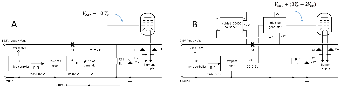
Figure 8.1 Principle of the standard grid supply of the uTracer (left), and the principle of the grid loupe (right).
The main problem in making a grid bias supply circuit that is able to deliver positive grid biases is that Vsup is already - apart from the anode and screen voltages - the highest voltage in the circuit. So there is no supply voltage to drive the circuit from. The problem is solved by using a small integrated isolated DC-DC converter (Fig. 8.1 right). This converter is powered by the supply voltage and generates a DC voltage that is isolated from the input so that it can be stacked “on top of” Vsup. Together with ground we have now created the positive and negative supply voltages the grid bias circuit needs to accurately generate voltages around Vsup.
The circuit
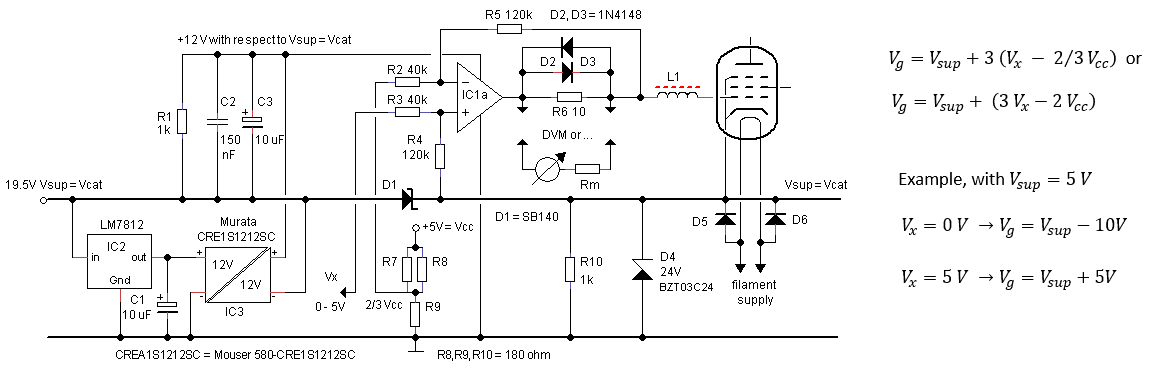
Figure 8.2 The circuit of the grid loupe.
Figure 8.2 shows the implementation of the circuit. The circuit uses the CRE1S1212SC isolated DC-DC converter from Murata. This tiny component takes a 12V voltage at the input, and generates a second isolated 12V voltage at the output. It costs only 4 euro and is readily available from Mouser. The maximum output current is 80 mA, which perfectly fits our application. The output is reasonably regulated, but a bit tricky and hidden in the datasheet, is that it needs a minimum load current of 10 mA, otherwise the output voltage will be way too high. A standard LM7812 was used to lower the 19V supply voltage to the 12V required for the CRE1S1212SC.
A slightly complicating factor is that the output of the low pass filter that turns the PWM signal from the PIC into a DC voltage is not only dependent on the duty-cycle of the PWM signal, but also on the amplitude, and thus to the +5V supply voltage of the PIC. From experience I know that there can be a variation of several hundreds of millivolts from one LM7805 to the other, and on top of that the output voltage will vary with load. The grid bias generator circuit therefore has to take these variations into account. It does so by realizing the equation shown on the right hand side of Fig. 8.2. The example shows that when the duty cycle of the PWM signal is 0% (Vx = 0V) the grid bias is -10V. When the duty cycle is 100% (Vx = Vcc) the grid bias is +5V. By involving Vcc into the equation we assure that the most sensitive range around Vg = 0V is always referenced to Vcc.
The heart of the grid bias circuit is OpAmp IC1a. Ignoring R6 for the moment, we see that it is configured as a Differential Amplifier with a gain of 120/40 = 3. The positive input of the differential amplifier is connected to Vx, while the inverting input is connected to a voltage divider that is set at 2/3 Vcc. The impedance of the voltage divider is low compared to the resistances in the differential circuit so that changing currents in the OpAmp circuit do not significantly affect the 2/3 Vcc reference. Circuits like this that operate near unity gain are always prone to oscillations, especially with capacitive loads. For this reason, the relatively old LM358 OpAmp was used because has a low bandwidth, and is unconditionally stable. Besides this, it is dirt cheap which is great if the OpAmp needs to be replaced “after an accident.”
Resistor R6 was added to be able to monitor the grid current. Assuming the current through R5 to be negligible compared to the grid current, the voltage drop over R6 will be directly proportional to the grid current. By placing R6 inside the feedback loop, the circuit will compensate for the voltage drop over R6. The grid current can simply be monitored by connecting a DVM over R6. The current is the voltage measured divided by ten, e.g. 100 mV corresponds to 10 mA. Alternatively, a sensitive mechanical Galvanometer can be used. In this case diodes D2 and D3 protect the galvanometer by clamping the voltage over R6 to +/- 0.8V. The value of Rm depends on the sensitivity of the meter used.
The circuit can source up to 32 mA of grid current, and is stable for capacitive loads up to 2 nF, which should be good enough for most tubes. Most control grids are made from ultra-fine metal wire, and not designed to conduct significant currents. The current limit of 32 mA therefore protects the tube somewhat from damage. Should a higher grid current be needed, then it can be easily doubled by “piggy backing” two LM358’s! A rather dirty and simple trick, but is works perfectly.
Construction of the grid loupe
To make the construction of the grid loupe as straightforward as possible the additional hardware that needs to be build is shown in the top schematic of Fig. 8.3. The red letters indicate the connections that have to be made to the uTracer hardware and refer to the corresponding letters in the bottom to schematics of Fig. 8.3. They are:
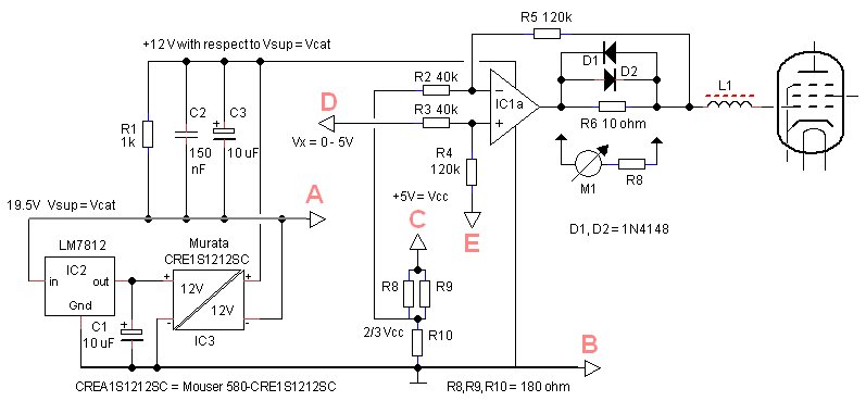
Figure 8.3 The complete circuit diagram of the grid loupe (top) with indicated the connections that have to be made to the uTracer circuit (bottom)
The circuit can be easily constructed on a small piece of perfboard. Figure 8.4 shows my implementation. I used a second 4 position terminal block of which the anode, screen and cathode terminals are looped to the original terminal block, but where grid terminal is connected to the grid loupe. Alternatively, a simple switch can be used to select either the standard grid supply or the grid loupe.
It is a good idea to add a small heatsink to the LM7812 regulator since it can become somewhat hot. To prevent the circuit from oscillating it is important to best to use an “old” relatively slow and unconditionally stable OpAmp like the good old 741 or the LM358 that I used. For this application they are perfect and it doesn’t make any sense to try to find something better (and more expensive).
The grid loupe circuit can be used in combination with the standard uTracer hardware (300 V and 400 V versions), as well as the low voltage hardware described in the previous section on this page.
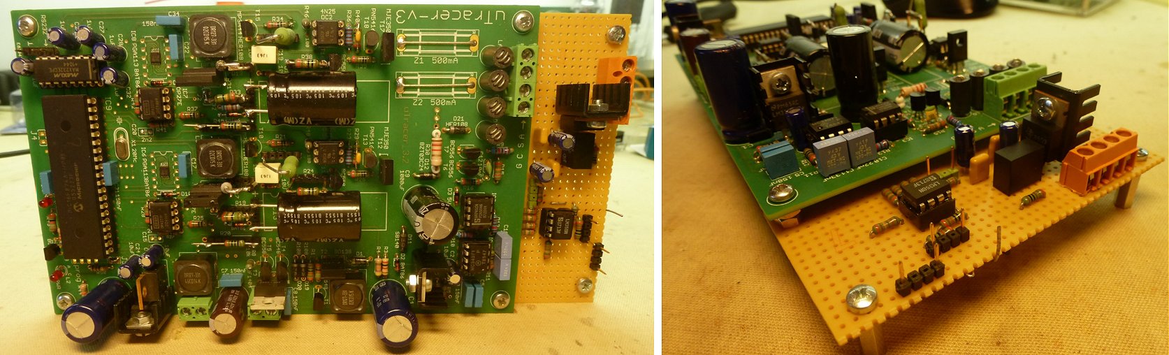
Figure 8.4 My implementation of the grid loupe circuit. Click here to view the other side of the board.
Adaptions to the user interface (GUI)
In total there are now three hardware versions of the uTracer: 1. The original 300V uTracer, 2. the 400V uTracer3+, and 3. the low voltage uTracer-LV described in the previous section of this Notebook. The grid loupe circuit described in this section can be used with all of the uTracer hardware versions. In order to have one GUI that can be used for all hardware versions including the grid loupe option the GUI 3.12.3 beta release was made that is based on the 3.12.2 release.
To select the grid loupe option, a tick box has been added in the main form (Fig. 8.5). Ticking this box will first of all reset the GUI and adjust the minimum and maximum grid voltages to -10 to 5 V respectively. Now -10 V grid voltage is translated to a grid output PWM signal with 0% duty cycle, while 5 V is translated to 100% duty cycle. De-ticking the box will again reset the GUI and return the minimum and maximum values back to -50 to 0 V.
Figure 8.5 The main form of GUI version 3.12.3
On the calibration form a “radio button” has been added to select the low voltage-LV hardware described in the previous section. After selecting another hardware version, the user should press the save button and restart the GUI.
A number of changes have been made to the calibration sliders on the calibration form to allow for the calibration of the grid loupe hardware. First of all the “Vsat” slider has been removed. This calibration parameter was intended to compensate for variations in the saturation voltage of the KSA1156 high voltage switch transistors. Secondly, the calibration sliders for the normal grid bias supply have been grouped more logically. Finally, 2 additional sliders have been added to allow for the calibration of the loupe hardware. The calibration procedure is very simple:
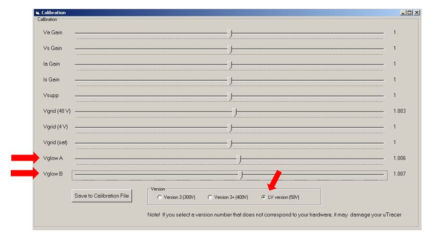
Figure 8.6 The calibration form of GUI version 3.12.3
To download the beta release 3.12.3 go to www.uTracer.nl and click Downloads > Beta Releases, or directly click here. To run the beta release you must have the current GUI release installed and running. You can then simple unzip the GUI 3.12.3 executable and place the executable in the same directory as the current GUI (for more info FAQ 5).
Experiments
To play with the grid loupe the same set of double triodes was measured that was also used in the previous section. Figure 8.7 shows the complete set of measurements. Each row shows a different tube type. The first two columns of graphs show low voltage measurements made by the low voltage uTracer in combination with the grid loupe. The first column is Ia(Vg) for grid voltages from -2 to +1V for Va=6.3, 12.6 and 20V. The middle column shows the low voltage output curves Ia(Va) for anode voltages from 0 to 20 V, for grid voltages ranging from -1 to +1V. The right column shows the output curves for normal anode voltages.
First of all, we see that even with a slight positive grid bias quite reasonable anode currents are obtained that are in the same order of magnitude as for normal anode voltages. Next to the first column the maximum grid current is noted. Since the anode voltage is pulsed, this is the anode current for Va = 0V. This is a kind of worst case situation because during normal use an anode voltage will be applied that will draw electrons away from the grid and reduce the grid current. Grids are made of extremely fine wire, which combined with the fact that they are suspended in vacuum, makes that they can only conduct very small currents. For most of the tubes a grid current of several mA didn’t seem to be a problem, however, for the low voltage car radio tube ECC86 is appeared to damage the tube.
Comparing the output curves at low voltages (middle column) to the output curves at normal anode voltages (right column), we see that the shape of the curves is completely different. Instead of the familiar triode shaped curves we find curves that look much more pentodes. I can very well imagine that at very low anode voltages and positive grid bias, the amount of electrons that is being swept away from the cathode is much more determined by the nearby grid, than by the distant slightly positive anode. In other words, the anode current only slightly depends on the anode voltage. I am not a “tubeologist” and far from an amplifier expert, but I can imagine that, despite the fact that reasonable currents are drawn at slightly positive grid biases, this will greatly effect “the sound” of the tubes.
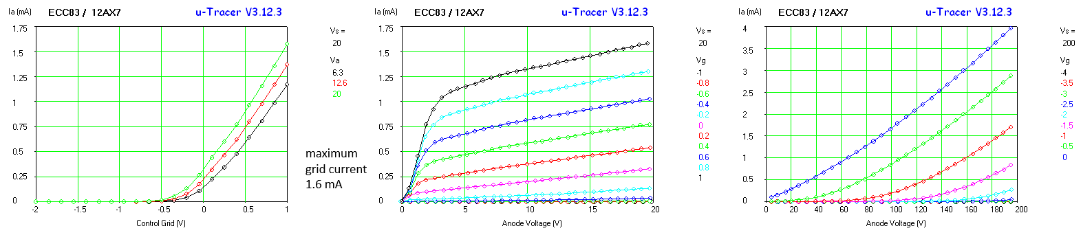
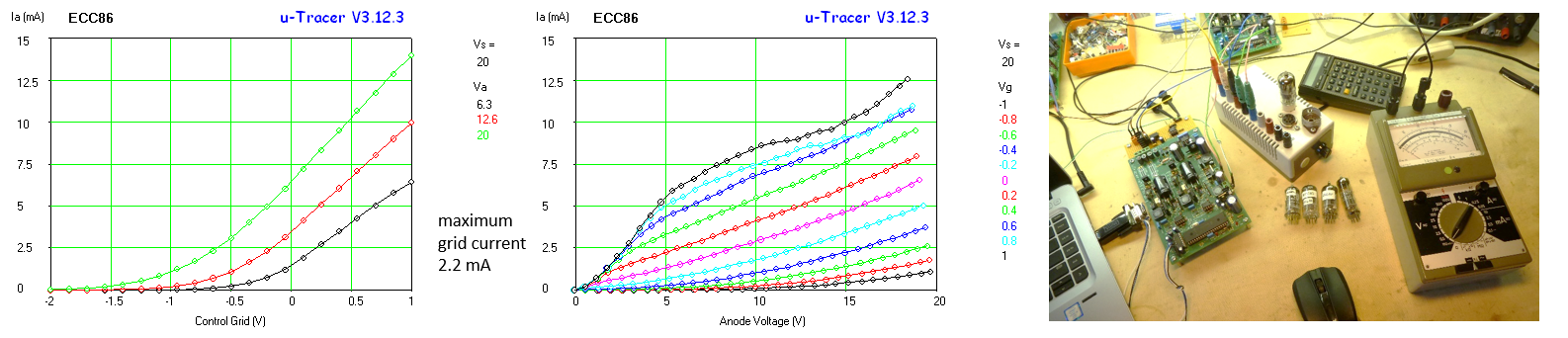
Figure 8.7 Ia(Vg) and Ia(Va) curves for a set of double triodes measured at low anode voltages and positive grid bias. The Ia(Va) output curves are compared to the output curves at normal anode voltages. The tubes characterized are: ECC83 (12AX7), E188CC (6DJ8), ECC85 (6AQ8), E90CC (CV5214) and the ECC86 (6GM8).
The phenomenon of grid current was studied a bit more in detail in Fig. 8.8. In the left graph a set of output curves is drawn for an E188CC for grid biases ranging from -0.2V to +1.0V. Next to the curves the maximum grid current (at Va = 0V) is listed. In the right hand graph, the decrease of the grid current with increasing anode voltage is shown. Extensive measurements on the triodes I had at hand showed that regardless of the triode type of the grid bias, the grid current approximately halves van the anode voltage is increased from 0 to 12 V, after which it remains more or less constant.
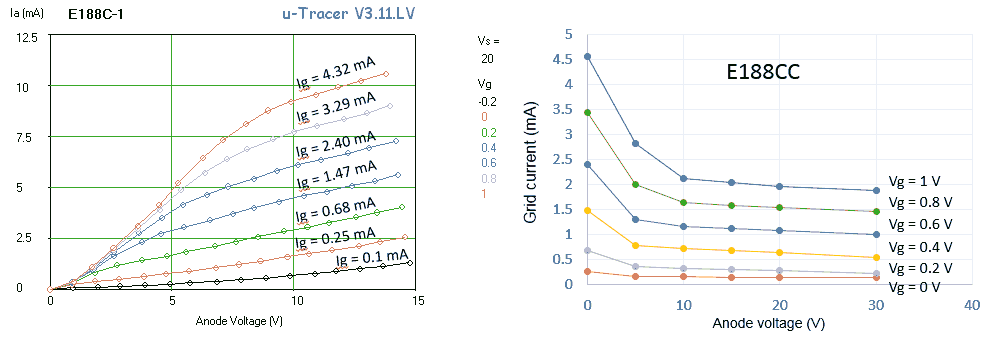
Figure 8.8 Output curves of an E188CC at positive grid biases with the maximum grid current listed (left), decrease of grid current with increasing anode voltage (right).
Almost immediately after I published the previous section I realized that there is quite an elegant way to actually record the grid current during the measurement. People playing with positive grid biases will, in the majority of cases, do this using triodes. This leaves the screen channel of the uTracer unused! The idea is to use a simple circuit that sinks a current from the screen channel of the uTracer that is equal to the gate current.
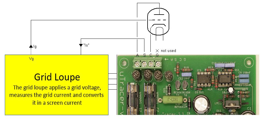
Figure 9.1 Basic idea of the new grid loupe circuit.
Figure 9.1 illustrates the basic idea. Like before the anode and the cathode of the triode are connected to the original anode and cathode terminals of the uTracer, and the grid of the tube is again connected to the grid loupe circuit. The grid loupe circuit however now has a second connection that is connected to the unused screen terminal of the uTracer. During the measurement a positive bias of e.g. 20 V is applied to the screen terminal, and the grid loupe circuit now sinks a current from the screen terminal that is equal to the grid current. So when the screen current is plotted, it is actually the grid current. The trick of course only works for triodes or pentodes that have been connected as triode.
The circuit
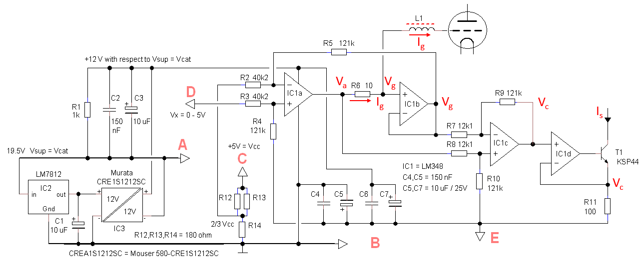
Figure 9.2 Circuit diagram of the grid loupe circuit.
Figure 9.2 shows the circuit diagram of the new grid loupe circuit. The basic idea of the circuit is identical to the old grid loupe circuit (see previous section). Going from left to right we see that the way the grid bias is generated has remained essentially the same. The only modification is the introduction of a 1x buffer (OpAmp 1B) in the feedback loop of OpAmp 1A. In the old circuit, the current flowing through the current sense resistor R6 included also the current in the feedback loop of OpAmp 1A through R5. In some cases, this current can be as high as 100 uA and is thus in most cases compared to the grid current itself. The buffer circuit around OpAmp 1B correct this flaw in the original circuit. Because of the very high input impedance of the OpAmp the current trhough R6 is now really only the grid current.
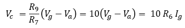
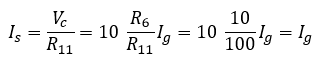
The circuit around OpAmp 1D and T1 is a simple voltage to current converter. T1 is used as an emitter follower so that the emitter follows the base voltage minus the emitter-base voltage drop of ca. 0.8V. So, when the output voltage of the OpAmp varies, the current through R11 varies proportionally. The voltage drop over R11 is fed back to the OpAmp so that the OpAmp will adjust its output in such a way that the voltage drop over R11 will be equal to Vc. Since the base current of T1 is negligible compared to the emitter current, the collector current will be approximately equal to the emitter current, and thus proportional to Vc. The equations above give the exact relationship. Note that with R6 set to 10 ohm and R11 to 100 ohm, the collector current of T1 is equal to the grid current.
As you might have guessed the collector of T1 is connected to the screen terminal of the uTracer. To make the whole thing work the collector of T1 has to be connected to a positive potential. Since the collector current is dictated by the emitter current, the value of this voltage is not critical. The default value in the low voltage version of the uTracer of 20 V is a good choice. For T1 actually any npn transistor with a reasonable gain and Early voltage could have been used. By using the KSP44 high voltage transistor we make sure that an accidental high screen voltage value does not automatically results in the death of the transistor.
Testing and construction
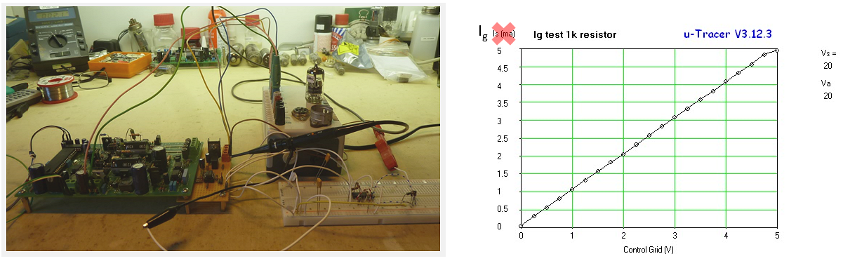
Figure 9.3 Breadboard testing of the new grid loupe circuit (left), response to a 1k resistor connected between grid and cathode terminals (right).
As usual the circuit was first tested on breadboard. The construction of the circuit poses no special problems. For the OpAmps an LM348 was chosen. This is essentially a quad LM741 OpAmp. I know that these OpAmps are old-fashioned, but they are slow and unconditionally stable (the last thing we want is an oscillating OpAmp) and on top of that very cheap. To obtain the 3x gain in the subtraction circuit around OpAmp 1A, I original used 40K (three 120k resistors in parallel) and 120k resistors. Martin manning suggested the use of 40.2k and 121k resistors because these are more or less standard values. The gain is then not exactly 3x but surely close enough. Since I didn’t have 40.2k resistors I used 39k with 1k2 in series. I used 121k and 12k1 resistors because they are used in the uTracer anyway.
The easiest way to test the circuit is to connect a 1k resistor between the grid and cathode terminals and make a Vg sweep from 1 to 5V. If everything if ok, this will result in a straight line from 0 to 5 mA (Fig. 9.3). Note that Is is plotted along the y-axis, but that it is in reality of course Ig.
Figure 9.4 New grid loupe circuit on perfboard. Click here, or on the picture for a high resolution photo of my note book with the layout details.
With the new circuit successfully tested a new perfboard design was made. I made a photo of the layout design for the perfboard version from my “real notebook” for people who would like to build the grid loupe circuit (Click Here). Note that the upper drawing shows the component side of the board and the lower picture the copper side. The letters refer the points in the uTracer circuit to which the grid loup circuit has to be connected (see Fig. 8.3). Finally, a test was run with the E188CC that was also used to produce the graphs in Fig. 8.8. As can be seen the grid loupe circuit reproduced the results although the exact shape of the grid current curves in reality is a bit different than what the limited manual measurement predicted.
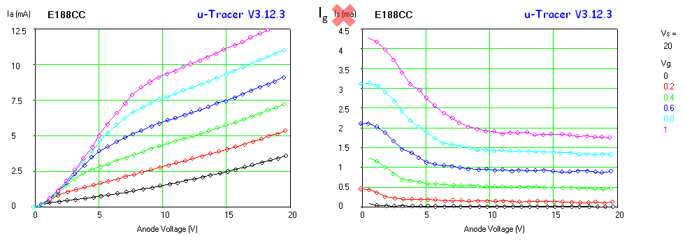
An E188CC measured for positive grid biases for comparison with Fig. 8.8
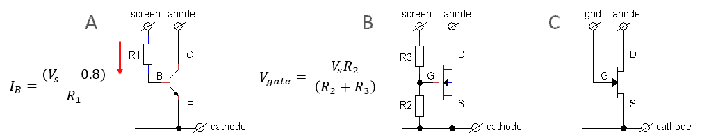
Figure 10.1 A few simple resistors turn the uTracer into a transistor tester.
Bipolar transistors are current amplifiers. The base of the transistor is supplied with a current, and as a result a larger collector current will flow. The ratio between the collector and the base current is called the DC current gain or Beta or hFE. The grid supply of the uTracer is not at all suitable to drive the base of bipolar transistors. First of all, it generates negative voltages and then again at near zero currents. However, it turns out that it is quite simple to convert the screen supply into a (near ideal) programmable current source that can be used to drive the base of npn transistors, the only thing that is needed is a resistor! Figure 10.1A shows the principle which makes use of the fact that the emitter-base voltage of a silicon bipolar transistor is almost constant between 0.7 and 1.0 V. A simple resistor can now be used to convert a screen voltage into a base current. If we program the screen supply to a series of not too small voltages, then the emitter-base voltage variation will be negligible so that the base current Ib = (Vs-0.8)/R. If Vs >> 0.8V this can be simplified to Ib = Vs/R.
The testing of an n-channel MOSFETs is just as simple. We again use the unused screen supply to generate positive gate voltages. To increase the accuracy of the gate voltage, a voltage divider is used to reduce the screen voltage by a factor of 10 so that the screen voltage range of 0 to 200 V translates to a practical gate voltage range of 0 to 20 V. Since the gate current is zero, a simple resistive voltage divider will be just fine. The only thing to take into account is that the impedance of the voltage divider is low enough to charge the gate capacitance well within the 1 ms measurement pulse. Measuring n-channel JFETs is even more simpler. In this case the grid bias of the uTracer can be directly used to drive the gate of the FET.
Circuit and construction
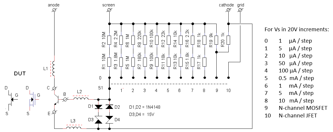
Figure 10.2 Example of an implementation of the transistor adapter module.
The concept translates into a simple circuit that most people can build for free after a dive into their junk box. In my case I was lucky to find a rotary switch with 11 positions (well actually 12, but I didn’t use the last one). Positions 0 to 8 of the rotary switch are used to select the desired base current range. More about the selection of the resistors R1 to R18 and the base current ranges at the end of this section. Position 9 of the rotary switch is reserved for the characterization of MOSFETs. The resistive divider consisting of R19 and R20 reduce the screen voltage by a factor of 10 before it is applied to the gate of the transistor. The odd value of 9k by the way, is obtained by placing a 10k, 100k and 1M resistor in parallel. Position 10 of the rotary switch is reserved for n-channel JFETs. In this case the negative grid voltage is directly connected to the gate of the FET. Most common (power) MOSFETs I know have a maximum allowable gate voltage of +/- 20V. To make sure that in case of a mistake the gate of the MOSFET under test is always protected, I inserted D1-D4. This tiny circuit clamps the maximum gate source voltage to +/- 15V (I didn’t bother to implement it).
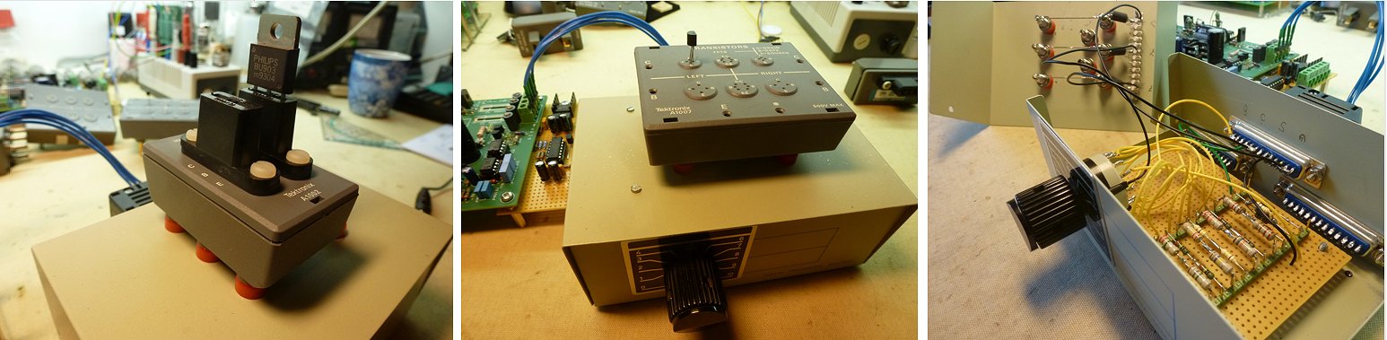
Figure 10.3 For the construction of the transistor test module and old RS232 port switch box was used. I was lucky to be able to lay by hands on a set of surplus Tektronix transistor fixtures which make it very convenient to use the tester.
Figure 10.3 shows my construction of the transistor tester adapter. I happened to have one of these old switch boxes that, before the arrival of USB, were used to switch between RS232 ports or printers. It is a nice and strong metal box with in the front panel already a hole for a rotary switch. In the back panel there are a few Sub D25 (RS232) connectors that were already there, and I used one to connect the box to the uTracer. I was very lucky to be able to put my hand on a collection of original Tektronix transistor test fixtures. These test fixtures came with the Tektronix 576 and 370B/371B curve tracers and were used to connect transistors in different packages to the curve tracer. The test fixtures have a set of “banana plug pins” on the back side that fit into connectors in the curve tracer. Since the Tektronix curve tracers where suitable for real power transistors, the fixtures use on the power terminals of the transistors two separate contacts, one for carrying the current and one for sensing the actually voltage on the pin of the transistor itself! We used to have quite a number of Tektronix curve tracers at different places in the labs at work. Most of them have gone except for a few (Fig. 10.5). Fortunately, there are still a few of the test fixture boxes lying around in odd corners and they came to good use for me!
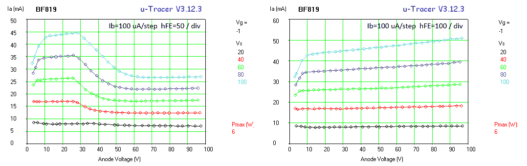
Figure 10.4 Left, typical result when the transistor oscillates for in a certain bias regime. In that case the uTracer will also often give compliance errors. Right, the transistor could be silenced with a few simple RFI ferrite beads.
The adaptor circuit proved to be quite prone to oscillations. Oscillations are a common problem in transistor curve tracers (read more here). Figure 10.4 shows a trace of a BF819, a 90MHz fT, 250V line driver transistor that was used in colour televisions. The left trace in Fig. 10.4 shows erratic behaviour at medium currents. At high currents the curves look normal. What happens is that for the medium currents the transistor is biased for maximum fT and will tend to oscillate. For higher currents the transistor is driven into (quasi) saturation resulting in a sharp decrease of fT and as a result the oscillations subside. A few ferrite RFI beads in the leads to the transistor were sufficient to stop the oscillations (Fig. 10.4 right).
Conventions and Beta
I spent the first part of my career at Philips Research developing new high speed / low power bipolar transistors for mobile communications. We had excellent facilities in those days, not only with for fabrication, but also for characterization. Although we were equipped with the newest HP parameter analysers like the HP4145, the first tests were always done with a Tektronix curve tracer like the 576, connected to the needles of a wafer probe station. No piece of equipment can give you so quickly an impression of the most important transistor parameters as an analogue curve tracer. Especially the breakdown voltages of a junction can be very quickly and reliably determined by slowly cranking up the junction voltage while observing the junction current. We do not make transistors anymore at Philips, but we still have a few curve tracers to quickly check the MEMS devices we make for medical applications. A colleague of mine still cherishes an old Tektronix 370B. When I powered it up for the sake of the writing of this article, it worked flawlessly after all those years (Fig. 10.5).
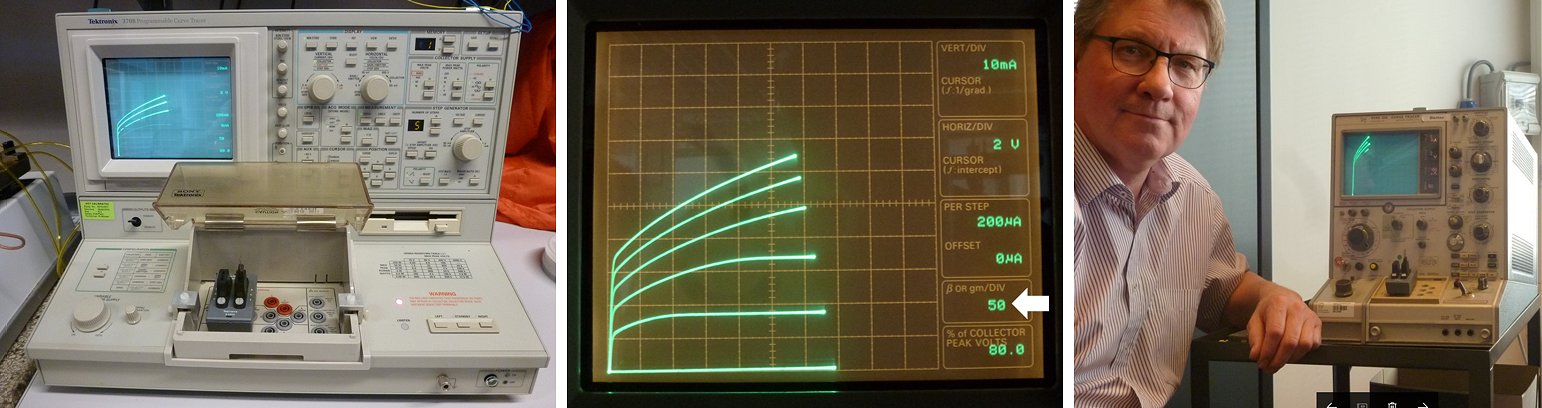
Figure 10.5 A relatively modern Tektronix 370B curve tracer (left) and yours truly next to his beloved 576. Because the curves are scanned, a complete set of curves can only be obtained using a long shutter time (middle).
The arrow in the middle picture shows the “Beta/division” feature.
One of the very useful features of the Tektronix curve tracers is a provision to directly read one of the most important transistor, the current gain or Beta, directly from the curves. The way it works is as follows, first you select the base current increments and the vertical collector current scale in such a way that you have the transistor biased in a regime that is relevant for your measurement. Now the curve tracer internally divides the collector current per division selected for the vertical axis by the base current step. This results in a “Beta per division” which is displayed in a separate window (Fig. 10.6 middle). To determine the Beta of a transistor in a certain part of the curve, you simply estimate the number of vertical divisions between two consecutive traces. In the example shown in Fig. 10.6 for example the current gain for small currents is approximately 90 while it quickly drops to less than 40 when the transistor is driven into saturation.
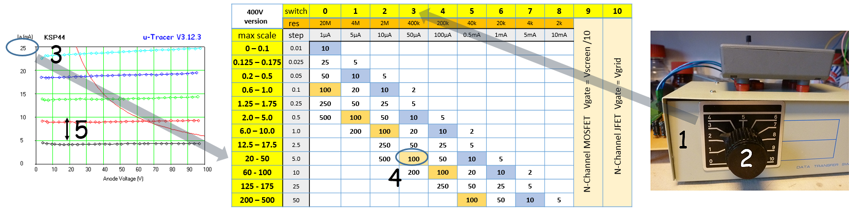
Figure 10.6 To find the Beta: 1. Do the measurement and find the proper base current range; 2. Read the base current selector position; 3. Read the maximum collector current; 4 look-up the Beta / division; 5 compare the distance between two curves with division size. The table can be downloaded here.
For my transistor tester I wanted to implement the same “Beta gadget.” To be able to do that, I made the convention with myself to only measure the bipolar transistor curves using 20V increments for the screen voltage, so: 0,20,40,60,80 etc. In that way I always know what the base current will be for every position of rotary switch. For example, with the resistance values used in the schematic in Fig. 10.2, the Ib increments with 1 uA with the switch in position 0; with the switch in position 1 it will be 5 uA; with the switch in position 2 it is 10 uA, etc. In order to calculate the Beta per division, however, we also need to know the collector current per division along the y-axis. A nice feature of the GUI is that it auto-scales the y-axis so that the axis and the number of divisions always have a pleasant appearance. This does complicate matters a bit however, since not only the maximum y-axis value, but also the number of divisions changes all the time. Fortunately, the number of divisions of the y-axis is fixed for every maximum value of the y-axis. So if we know the maximum y-axis value, the current per division is known. To determine the Beta / division a simple table can be used.
The procedure is explained in Fig. 10.6: First measure a set of curves with Vs in 20V increments. Then after the measurement read the maximum y-axis value. Look up in the table the Beta per division. Verify that in the measurement in Fig. 10.6 the beta is approximately 100.
Examples
 To measure a set of bipolar or n-channel MOSFET output curves the I(Va,Vs) measurement type is selected. Below, by way of illustration, some measurements on some high voltage transistors I had lying around are shown.
The BF819 is a video output transistor with a gain of approximately 100. When we developed transistors, 100 was always the target value for the Beta. A lower value makes circuit design more difficult, while higher values unnecessarily decreases the collector-emitter breakdown voltage. At currents above 100 mA we clearly see (quasi) saturation effects for the BF819.
To measure a set of bipolar or n-channel MOSFET output curves the I(Va,Vs) measurement type is selected. Below, by way of illustration, some measurements on some high voltage transistors I had lying around are shown.
The BF819 is a video output transistor with a gain of approximately 100. When we developed transistors, 100 was always the target value for the Beta. A lower value makes circuit design more difficult, while higher values unnecessarily decreases the collector-emitter breakdown voltage. At currents above 100 mA we clearly see (quasi) saturation effects for the BF819.
The KSP44 is the high voltage npn transistor used in the uTracer to discharge the 100uF reservoir capacitors. In Fig. 10.8 A and B the KSP44 is traced in its normal operating regime. In Fig. 10.8 C the same transistor is driven far beyond its maximum power dissipation limit. Of course this is possible because of the pulse measurement principle of the uTracer. Nevertheless, the safe operating area (SOA) still has to be taken into account, even for pulsed measurements. If we look at Fig. 8 of the datasheet of the KSP44, we see that the SOA is specified for different pulse lengths. At 1 ms - the uTracer pulse length - the maximum permissible current at 300V collector voltage is about 30 mA. Looking at Fig. 10.8 C we indeed see a tendency for the collector current to run away around that value.
The BU903 traced in Fig. 10.9 is a real monster with a breakdown voltage of 550V, a maximum current of 6A and a maximum power dissipation of 125W! As usual with these power transistors they have a low hFE to make them resistant against base punch-through. The datasheet specifies a minimum value of hFE=8 which is in excellent agreement with the measurement. In Fig. 10.9 B the BU903 is tested to the limits of the uTracer (but by far not to the limits of the transistor).
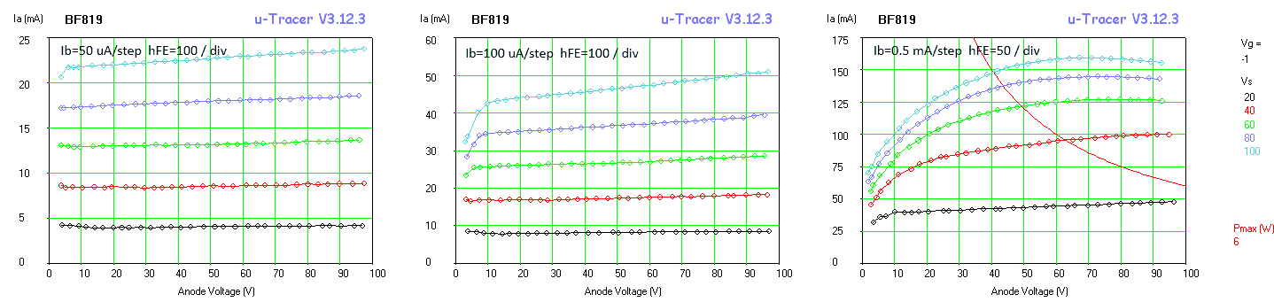
Figure 10.7 BF819 video transistor (BVceo=250V, Imax=300mA, Pmax=6W, fT =90MHz)
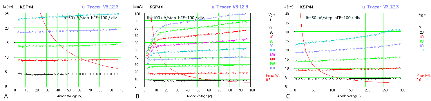
Figure 10.8 KSP44 general purpose HV transistor (BVceo=400V, Imax=300mA, Pmax=0.625W)
Figure 10.9 BU903 TV deflection transistor (BVceo=550V, Imax=6A, Pmax=125W)
Some considerations
As mentioned, I made for myself the convention to measure the transistors with 20V screen voltage increments: 20,40,60,80,100,…. Unfortunately, the uTracer is not so good in accurately generating very low anode and screen voltages (read more in the weblog or on this page). So in principle (and also in practice) it might have been better to take e.g. 50V increments, and increase the base resistors proportionally by a factor of 2.5. However, I wanted to use the transistor test adaptor also in combination with my low-voltage uTracer. The low-voltage uTracer can only generate voltages up to 50V, so the choice for the resistor values given in Fig. 10.2 is a compromise. If you are planning to only use the transistor adaptor in combination with the normal high-voltage uTracer3+, you can obtain a little bit better results by using e.g. 50V increments and increasing the base resistors with a factor 2.5. To illustrates this Fig. 10.10 shows next to each other a set of KSP44 curves measured with 20 V increments (Fig. 10.10 A), and a set of curves with 50 V increments (Fig. 10.10 B). The curves in the latter figure are definitely smoother. For comparison I have also included a set of curves taken with the low-voltage uTracer, which are again significantly better. Enthusiasts who want to modify the “Beta look-up table” can download the original pptx here.
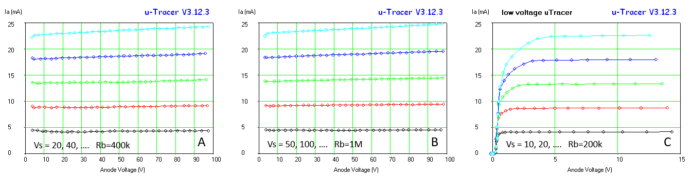
Figure 10.10 KSP44 output curves with: A) the circuit of Fig. 10.2 and 20V Vs increments and Rb=400k; B) Vs increments of 50V and the Rb increased to 1M; C) using the low-voltage uTracer.
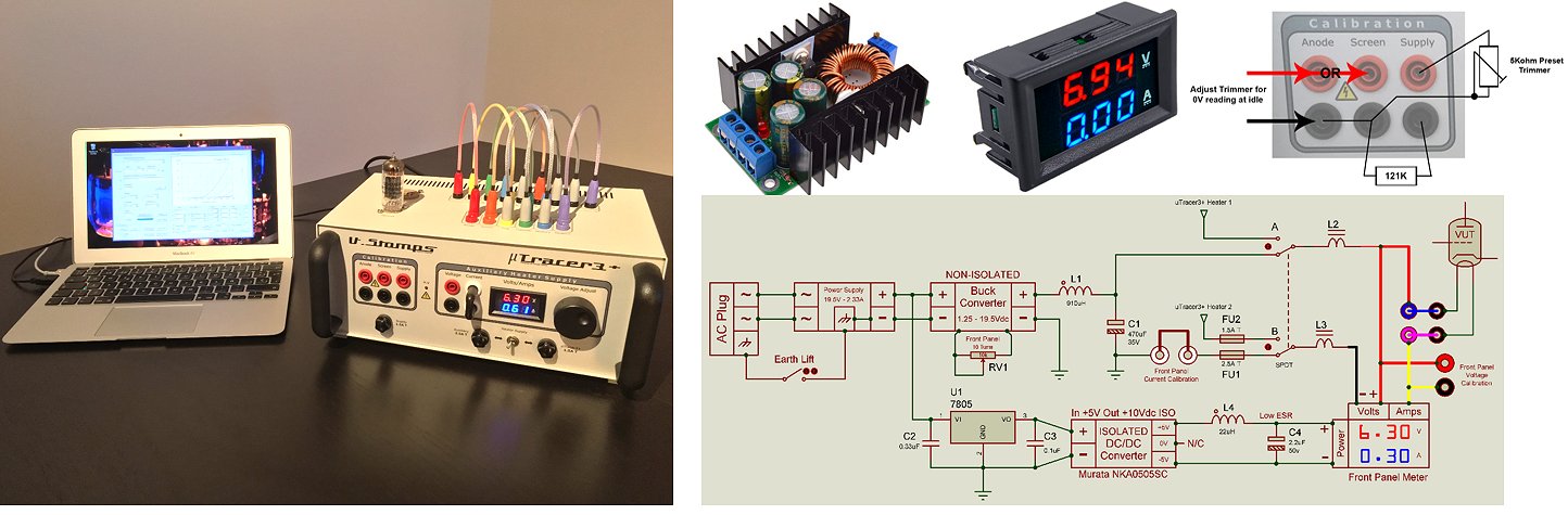
The Quicktest
Ok, now that we know that the plate resistance is nothing else than the inverse slope of the tangent to the output curve at a certain bias point, the next question is how to automatically construct such a tangent? The simplest way, and indeed the method used in the quicktest, is to measure the anode current in two points a and b on either side of the bias point Vx (Fig. 12.1 A), and then to mathematically construct a straight line through these points. The inverse of the slope of this line is the anode resistance in Vx. In the quicktest you can specify the distance of a and b from the bias point Vx with the “stepping variables” that can be entered as a direct voltage value, or as a percentage of Vx.
Here already the problems start, “what is the optimal value of the distance of a and b to Vx?” Mathematically speaking we would like to choose a and b as close to Vx as possible. However, although the measurements are represented at a drawn line, they are in reality nothing more than a number of discrete measurement points interconnected by pieces of line (Fig. 12.1C). Unfortunately, measurements are always subjected to noise and on top of that the AD converted that is used to measure the currents has a finite resolution and also the accuracy by which voltages can be set is limited. So the closer a and b are chosen to Vx, the larger the inaccuracy in the anode resistance.
The higher the anode resistance the more difficult it becomes to determine the anode resistance with any reasonable accuracy. Figure 12.1B shows a tube with a higher output resistance compared to Fig. 12.1A. Note that for the same variation in anode voltage the change in anode current has decreased. At a certain point the variation as a result of noise or ADC quantization will start to dominate (Fig. 12.1C) and the measurement will become meaningless. For this reason, the maximum value for the anode resistance that will be displayed in the quicktest has been clipped to 1M.
Note the quicktest feature uses exactly the same method to determine the transconductance(s), only in this case control grid voltage and the screen voltage are stepped.
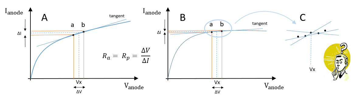
Figure 12.1 Determination of the anode / plate resistance.
Curve fitting
Next to the curve for the anode current as a function of anode voltage, we sometimes also would like to plot the anode resistance as a function of the anode voltage. With the method described above, this would inevitably result in very “noisy” curves. As an alternative approach, I therefore implemented a method that is based on curve fitting. The idea is very simple: a polynomial is fitted through the measurement points which as accurately as possible follows the measurement points, but averages out the noise. Once the factors of this polynomial are known, the curve can be differentiated analytically, resulting in a smooth anode resistance curve.
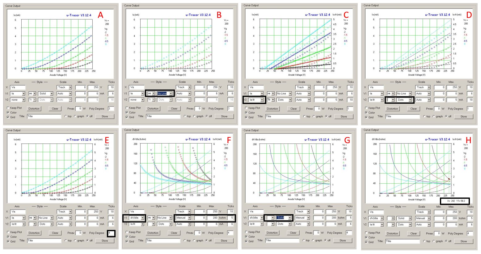
Figure 12.2 Step-by-step explanation of the curve-fit method to extract resistance curves.
This example shows the extraction of a set of anode resistance curves of an ECC83 (12AX7), the extraction of a set of transconductance curves is done exactly in the same way.
The curve fit concept is step-by-step illustrated in Fig. 12.2. This is how I do it:
Obviously the success of this method is highly dependent on the quality of the fit of the polynomial to the measured curve. I didn’t build-in in the GUI a means to assess the quality of the fit. To be honest, before the uTracer (or any other tube-curve tracer) the only means to determine the tangent would have been to draw the output curves and then “on the eye” construct it. So I think judging the quality of the fit “ŕ vue” will be good enough.
A bit of a tricky thing is the selection of the proper polynomial degree. A too low degree will obviously result in a bad fit. However, a too high degree is also not desirable. The higher the degree, the more the polymonial wants to follow the data points. Remember that if the degree of the polynomial equals the number of datapoints, the curve will go through all points! Obviously we don’t want that, because we will then have the same problem as before, but in this case it will not result in a “noisy” plate resistance curve, but in “oscillations” in the curve (see example in the next sub-section)!
An example, the EF86
I received a question from Brice Hamon who had difficulty in determining the plate resistance of an EF86. Personally I am not into audio amplifiers, but apparently the EF86 is widely used by audio enthusiast. The tube is especially designed for audio applications as it has low noise, hum and microphony characteristics (Click here for a datasheet). The tube also has a very high plate resistance that is in the datasheet specified as 2.5 – 3 Mohm! In view of what I have written above on the limitations of the quicktest, it is not surprizing that the quicktest returned a “> 1Mohm” value. I suggested Brice to use the curve-fit method, but also that turned out to be less straightforward than I expected.
Figure 12.3 Brice’s original result (left) and a set of EL86 curves (right).
Figure 12.3 left shows the “plate curve-fit” Brice sent me. The plate resistance was full of oscillations, while another annoying fact was that the maximum value that could be set for the vertical scale was limited to 1000 kohm. The right graph in Fig. 12.4 shows an EF86 (to be honest it was a PF86 which is identical but has a lower heater voltage) I traced myself. The EF86 indeed has a very high plate resistance, especially for lower grid voltages. For Vg = -3 V, the curve is practically horizontal!
An easy thing to solve was the limitation for the maximum value that can be entered for the y-axis. At some point I had to set a maximum value and at the time I set it to 1000, not realizing that there were tubes with an even higher anode resistance. In the beta release starting from version 12.3.4 the maximum value that be entered in any field has been increased to 1000.000 which should be high enough for all reasonable purposes. Click Here to go to the beta release page for instructions how to download and install the beta release.
Now with respect to the curve fitting: the first thing to remark here is that for an optimal fit strategy it is in general a good idea to limit the fit to the part of the curves that is really of interest for the application. Fitting the whole curve with one fit will require a high order polynomial, which in turn will give rise to “oscillations” in the derivative (plate resistance). Looking at the right graph in Fig. 12.3 we may safely assume that the tube will not be biased in region a. The high voltage side of the characteristics additionally shows a strange small bump (region b) that also seems undesirable. So for the moment we assume that the practical bias regime will be 50 < Va < 200 V.
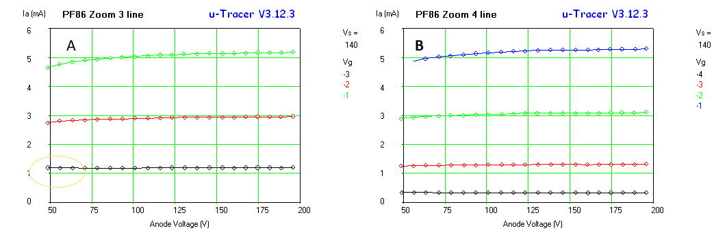
Figure 12.4 Close up of the relevant bias regime.
Figure 12.4A shows a close-up of the relevant bias regime. Of course these curves (and all other curves in this section) were made after setting the averaging manually to maximum (32x). Recording a full set of curves will take a bit more time, but the noise will be significantly reduced. When I took these curves, I noticed something odd: the first point of the first curve (encircled point) is always a fraction higher than expected. At the moment I have no idea what the cause is, and it is a thing I will look into later. For the time being, the “problem” could be solved by adding an extra curve taken at Vg = -4 V (Fig. 12.4B).
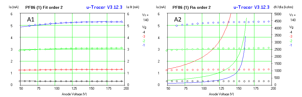
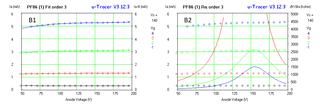
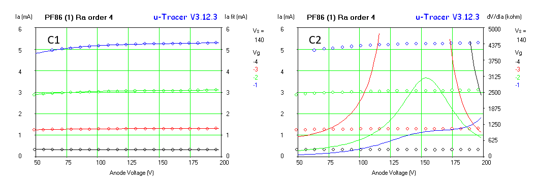
Figure 12.5 Anode current curve fit results (left column) and derived anode resistance curves (column right) for an EL86 and for polynomial orders 2 to 4.
Figure 12.5 shows for polynomial orders 2 to 4 the fit of the curves over the selected bias range (left series of graphs) and the extracted anode resistance (right series of graphs). At first sight, the current fit is very reasonable in all cases, especially for orders 3 and 4. For Vg = -4V and Vg = -3 V the curves are so flat that the anode resistance explodes. I don’t think given the measurement accuracy of the uTracer it makes sense to attach a meaningful interpretation to the values. For Vg = -2 and -1 V the results look more meaningful. The fact that all three order fits more or less give the same results, add confidence to the feeling that these values are realistic (apart from the fact that they very reasonably agree with the value given in the datasheet).
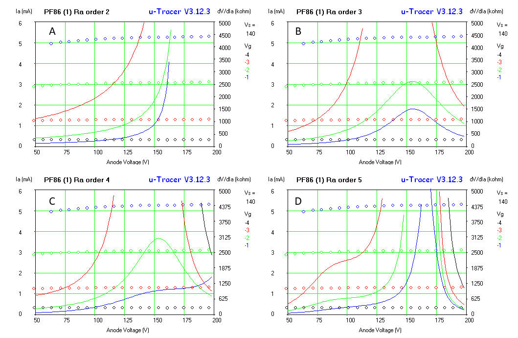
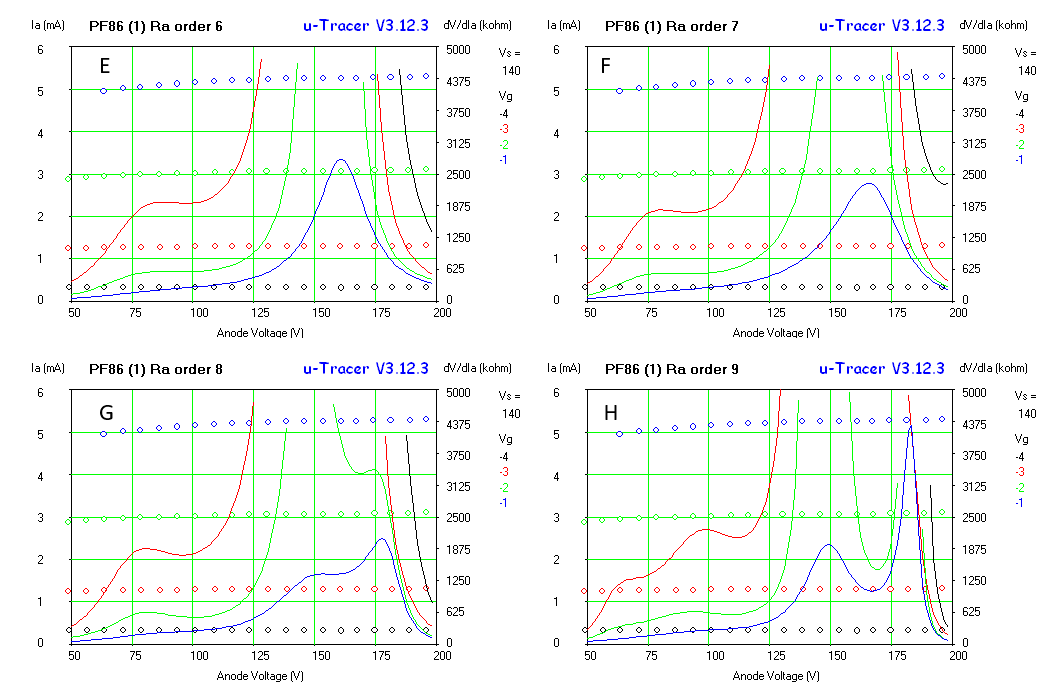
Figure 12.6 EL86 plate resistance curves for polynomial orders 2 to 9.
To illustrate that a higher order fit doesn’t automatically result in a more accurate determination of the anode resistance, I measured the anode resistance curves for orders 2 to 9 and put them next to each other in Fig. 12.6. Note that with increasing order the curves tend to start showing “oscillations”. What happens of course is that instead the fit no longer averages out all the irregularities in the curves, but that it actually starts following them. Something we were trying to avoid in the first place!.
In Summary
Accurately measuring the anode resistance of a tube like the EF86 pushes the performance of the uTracer to the limits of what it can do. Some people will immediately say “use an ADC with more bits.” It is ot as simple as that. Increasing the resolution of the ADC also requires a much more careful design of the whole circuit. It also requires a more accurate setting of the voltages which is difficult in the present circuit. The nice thing of the uTracer is, I think, that it exactly hits the sweet spot where very acceptable performance is combined with moderate-cost.
For most tubes, the curve-fit method to determine the anode resistance (and the transconductance) will work just fine, resulting in nice smooth curves. For tubes with a very high anode resistance in summary I recommend the following procedure:
 People who regularly restore vintage equipment will recognize that old electrolytic capacitors are always a source of trouble. Especially if the equipment hasn’t been used for a long time, these capacitors can be leaky or even shorted. It is therefore advisable to never directly switch on a piece of vintage equipment with an unknown history, but always first check the high voltage capacitors, especially in the power supply section. Failure to do so has on many occasions resulted in an exploding capacitor and an alarmed household.
Electrolytic capacitors
The heart of ordinary electrolytic capacitors is a thin aluminium oxide layer on one side of an aluminium foil that constitutes the anode of that capacitor. This aluminium oxide layer is grown in the factory by an electrochemical process, and it constitutes the dielectric of the capacitor. The cathode terminal of the capacitor is in fact a liquid electrolyte, usually an acid in an impregnated sheet of paper that is pressed again the surface of the aluminium oxide. The electrolyte in the sheet of paper is contacted by a second foil of aluminium, this time without oxide, to be able to connect the cathode to the outside world. The foil-paper-foil sandwich is rolled op and inserted in a metal can. The thickness of the aluminium oxide dielectric is proportional to the working voltage of the capacitor. So the higher the working voltage, the lower the capacitance density per unit area. This is the reason why for the same capacitance, high voltage capacitors are bigger than low voltage capacitors.
Unfortunately, the slightly acidic liquid electrolyte also very slowly etches the aluminium oxide. Under normal use this is not a problem. Every time when a voltage is applied to the capacitor it will re-start the electrochemical process that restores the dielectric to its original thickness. However, when a capacitor hasn’t been used for a very long time, its dielectric thickness may have reduced significantly resulting in a much lower safe working voltage. Additionally, small pinholes may have formed which may result in a significant leakage current. If no precaution is taken and the capacitor is directly connected to the maximum voltage, this may result in a significant dissipation of energy and subsequent heating and even exploding of the capacitor.
Forming electrolytic capacitors
Fortunately, it is very easy to check capacitors for their proper working. All that needs to be done is to limit the current for example with a high value resistor. In its simplest form you take a high voltage supply and connect that via a resistor of say 10 kohm to the capacitor, while the current is monitored. When the capacitor is ok, the current should quickly drop to a value in the tens of micro amp range. A 100 uF capacitor for example should be 99% charged in 3RC = 3*100E-6*10E3 = 3 seconds. In most cases, however, it takes a much longer to obtain a current in the micro-amp range. What is happening is that slowly the dielectric is being restored to its original thickness. It may very well be that a sufficiently low current is never obtained. In that case the damage to the capacitor was too large and it will need to be replaced. To maintain the original look of the instrument some people go as far as hollowing out the defective capacitor and filling it with a new replacement type. This is often possible since modern capacitors are much smaller that vintage ones. Capacitor development obviously also has seen a continuous innovation and you will find that capacitors from the seventies onward are much more stable and robust
So the good news is that in many cases old vintage capacitors can be brought to life by carefully applying a voltage to them while limiting the current. This process is called (re-)forming. There is no commonly agreed upon best strategy how to do this. Some people simply leave the capacitor in the circuit and power the piece of equipment via a variac and then slowly increase the power supply voltage. Others remove the capacitor from the circuit and connect it via a high value resistor to the maximum working voltage. At the end of this section after the examples, I have included some of the many links on capacitor formation that can be found on the internet.
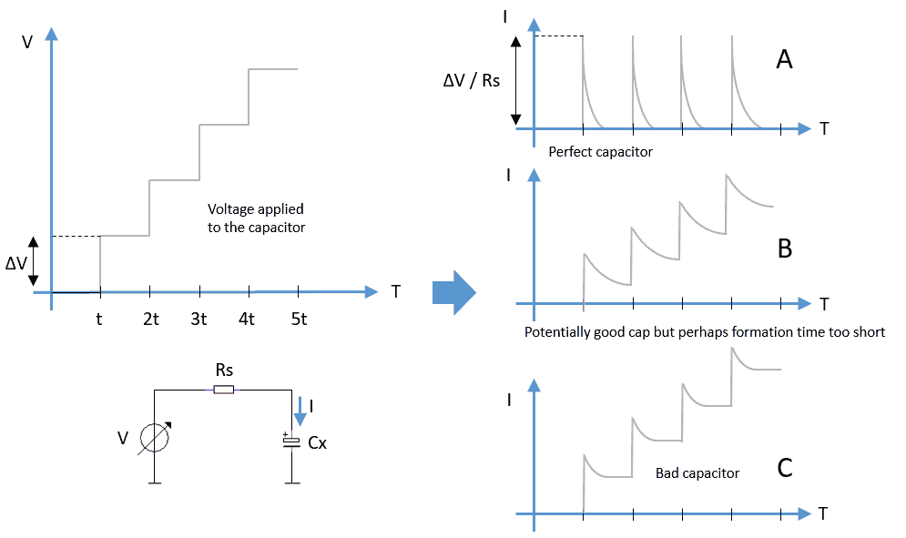
Figure 13.1 My personally preferred method of forming vintage electrolytic capacitators.
I personally favour a method where the capacitor is connected via a resistor to an adjustable voltage source whereby the voltage is increased in steps, while at each step the capacitor is given time to stabilize (Fig. 13.1 left). Depending on the state of the capacitor a variety of current responses is possible. In the right of Fig. 13.1 a selection of responses is sketched.
I have the strong impression, that even when the current has dropped to an acceptable low value, the oxide dielectric still continues to improve in quality (becomes denser), while the high voltage remains applied. The formation process can therefore easily take many hours. Apart from the fact that this “occupies” my lab high voltage supply, it is rather cumbersome to increase the voltage every (half)hour. So while I was looking for some way to automate it, it occurred to me that the uTracer had everything on board to do the job!
The basic circuit
It will be recalled that the anode and screen high voltage supplies of the uTracer consist of two low current programmable boost converters that charge the two 100 uF reservoir capacitors of the uTracer to the desired voltages. The boost converters can only supply a current of a few milliamps, which is more than enough to re-form capacitors!
Figure 2 shows the idea in its simplest form. The cathode of the capacitor to be reformed is connected to the cathode terminal of the uTracer, while the anode is connected, via a 10k resistor, to the anode of one of the 100uF reservoir capacitors of the uTracer. By specifying a delay in the “delay” field, the uTracer will charge the capacitors to the desired voltage and then hold that value before continuing to the next “measurement point.” Read more about the delay function here. Since the uTracer has two independent high voltage sources, it is possible to re-form two capacitors at the same time. Handy when reforming “combined” vintage electrolytic capacitors! The two “re-forming circuits” are obviously identical, so here I will only discuss one. Diode Da1 prevents current flowing back from the capacitor that is being reformed back into the uTracer which might disturb the voltage regulation of the circuit. Diode Da2 makes sure that the capacitor can never be revers biased. Current meter Ma is used to monitor the current. Personally I prefer an old fashioned dial instrument because it gives a better and faster idea of the progression of the current, but of course a digital current meter may also be used.
To operate the circuit, you:
Figure 13.2 The simples circuit to turn your uTracer into a capacitor re-former.
This circuit will leave the capacitor fully charged after the procedure! Read the warning below
This simple circuit idea works well, and it will re-form your capacitors, however, it is not very elegant for two reasons:
The “Deluxe” version
Although it is not absolutely necessary to record the current at the end of each step, it would be a nice feature especially since all the infrastructure to do so is present. The reason it doesn’t work properly with the simple circuit of Fig. 13.2 lies deep in the inner workings of the uTracer and isn’t easily explained. To understand it, you have to know that transistor T15 serves two purposes. First, after each measurement cycle it discharges the 100uF capacitor through R35 and D15 until a safe voltage is reached and the HV LED can be turned off. Note that when T15 is on, there is a voltage drop over zenerdiode D15 which charges C19 to 10V. This brings me to the second purpose of T15. The high voltage switch circuit consisting of T16,T17,T18 and OC2 is a “floating circuit.” The power it needs for its operation comes from C19. To be sure that there is enough energy stored in C19, the PIC pulses T15 for 10ms immediately before every measurement pulse (Read more here).
Obviously this will discharge the 100uF reservoir capacitor C18 a bit, but for tube measurements this doesn’t matter since the correct voltage is measured at the end of every measurement pulse anyway. However, in the circuit of Fig 13.2, since the voltage on the C18 is slightly lower than the voltage on the capacitor that is being reformed, diode Da1 will block and no current is measured.
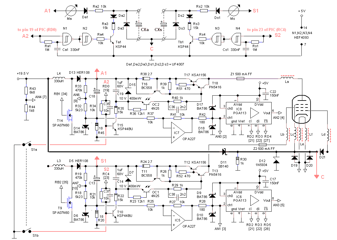
Figure 13.3 Deluxe uTracer capacitor forming circuit.
The solution to this is very simple. In Fig. 13.3 switch S1 has been added which, when closed, basically permanently switches off T15 (and T10) by connecting their basis to ground. This will obviously disable the high voltage switches, but they are not needed during the re-forming process anyway. Although accurate current measurement is now possible, the “re-forming capacitor” will still remain charged after a forming cycle. To also solve this, a small auxiliary circuit is needed. The circuit around Ra1, Ca1, N1, and N2 is basically a “time high-pass filter.” Only pulses longer than approximately Ra1*Ca1 = 1M*330nF = 330ms appear on the output of N2, while shorter pulses are blocked. The input of this filter is connected to the output pin of the PIC that normally drives T15. The result is that the short charge pulses that distorted the current measurement are blocked out, while the large discharge pulse at the end of each measurement cycle is passed through to Ta1, which now discharges both the forming capacitor as well as C15.
The circuit can easily be built on a piece of perf board and is operated in exactly the same way as the basic circuit described above and obviously also needs GUI version 3.12.5 (or higher).
Figure 13.4 The Deluxe circuit on breadboard during testing
Forming strategy and examples
As already mentioned, there is no commonly agreed upon re-forming strategy, but let me describe how I do it. The first thing I do is get an idea of the condition of the capacitor. Usually I make a limited voltage sweep with a delay of 5 to 20 sec while monitoring the current. Even if the capacitor is rated for 400V, I limit the sweep to 200 V maximum. This will already give a good impression of the state of the capacitor while staying on the safe side.
Fig. 13.5A shows such a sweep for a 100uF / 300V capacitor that hasn’t been powered since the moment is was manufactured. We see that the current quickly rises to 16mA for 180V! This already amounts to 3W of dissipation, which continued might dangerously heat the capacitor! So during these initial sweeps it is wise to keep an eye on the current meter and interrupt the measurement if needed. By the way, the standard uTracer will only supply currents up to 8 mA or so. When the circuit (capacitor) draws so much current that the boost converter cannot reach the set voltage, it will “hang” and display an error message on the GUI. I was using here a uTracer that has two inductors installed per boost converter (click here). This at least doubles the output current.
The next voltage sweep applied to this capacitor was again 20 to 200V, but now with 300sec delays (Fig. 13.5B). It is interesting to observe the current meter during the delays and see the current drop as the capacitor “heals” itself. The current plotted in the graph is obviously the current at the end of the delay. Observe that the currents are already much lower than in the initial sweep and that the current strangely enough saturates around 3mA. After this sweep, which already takes almost an hour, I again made a fast sweep to see if the capacitor had really improved (Fig. 13.5C). The low currents indeed show that this is the case as these currents were obtained in less than 5sec. With the currents now on the safe side, a new long sweep with delays of 300sec was made, but now up to the full specifies voltage of 300V (Fig. 13.5D). This was again followed by a fast sweep to check the progress (Fig. 13.5E). Observe that now especially the current at higher voltages has been reduced. This demonstrates that to properly form a capacitor you have to use forming voltages higher than the specified working voltages. I discussed this with a colleague at Philips who worked for a large part of his career in the electrolytic capacitor manufacturing site of Philips when it was still Philips. He confirmed that also during manufacturing electrolytic capacitors are formed at a 20% higher voltage than their specified working voltage.
Two further 300sec forming cycles at higher voltages further reduced the current (Fig. 13.5 F-I). This illustrates the effect of time. Clearly time is an important factor in re-forming capacitors and I wouldn’t hesitate to leave the capacitor at maximum voltage for a night. Fig. 13.5J shows the same capacitor after a week. The leakage current again strongly increased. However, a new forming cycle, now at maximum voltage for hours resulted in a more stable behaviour (Fig. 13.6K after 2 months).
Note that the first measurement point in a curve usually shows a somewhat higher current. I spend quite some time searching for the origin of this peculiar behaviour, but I didn’t find it. If you discover it I buy you a beer!
The final question is what leakage current can you allow for an electrolytic capacitor before you reject it? Again that is difficult to say. The editor of the site ElectroJumble gives the maximum values of leakage currents for capacitors that were sold by Radiospares in 1968. The table he shows based on the formula Imax = 0.05*C*V + 250, with Imax in microamps, C in uF and V in Volts. Ignoring the quarter milliamp, we see that as expected, the maximum leakage current is proportional to both C as well as V. As a rule of thumb, the maximum leakage current for a 100uF / 200V capacitor should be in the order of 0.05*100*200 = 1 mA. If you double the capacitance or double the voltage the maximum allowed leakage current doubles etc. etc.
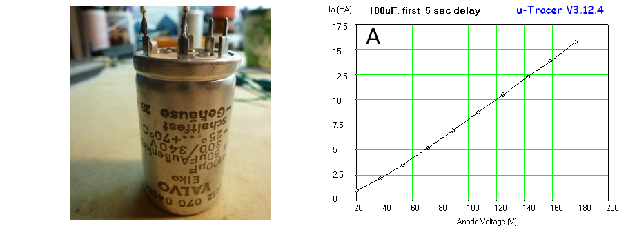
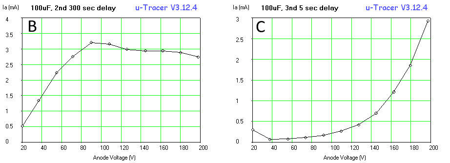
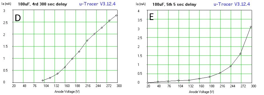
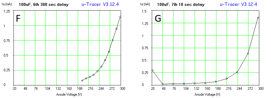
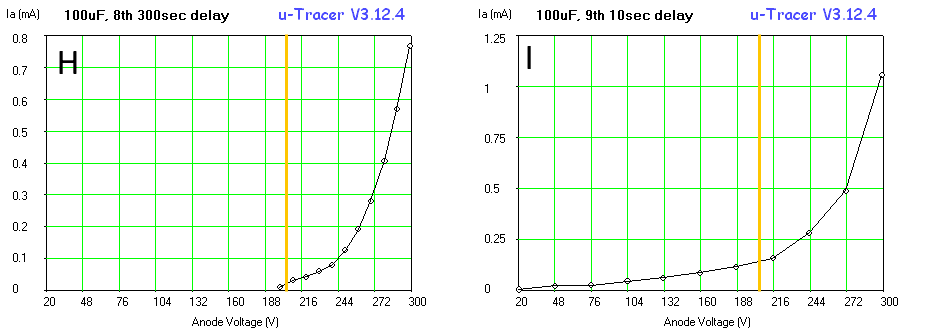
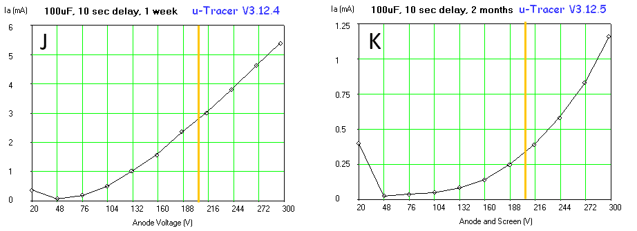
Figure 13.5 A 100uF / 300V vintage capacitor from VALVO (Philips Germany)
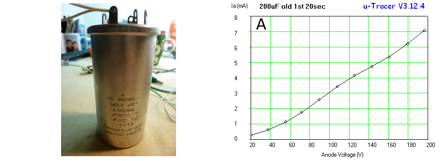
Figure 13.4 a 200uF / 300V capacitor from Loewe from the same time period as the previous one.
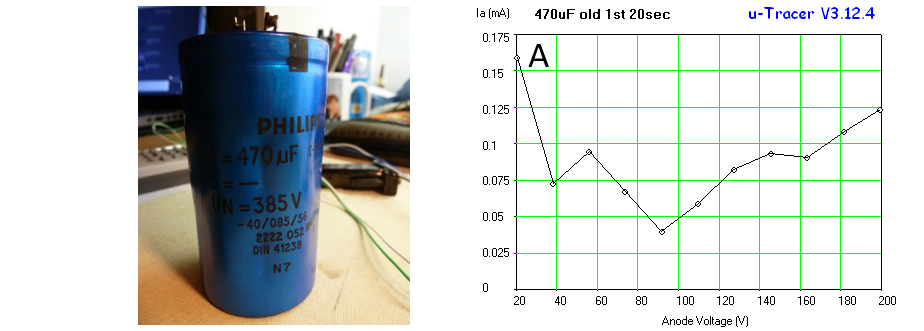
Figure 13.5 a 470uF / 385V capacitor from Philips from a later generation as the previous ones, probably the seventies.
Clearly the technology did improve significantly as the leakage currents are extremely low.
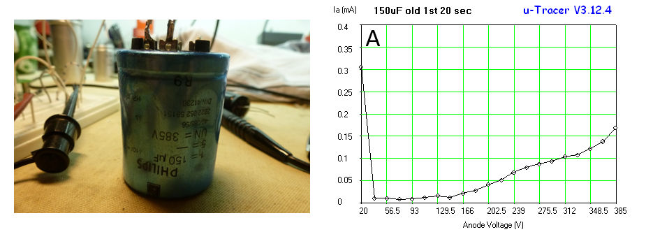
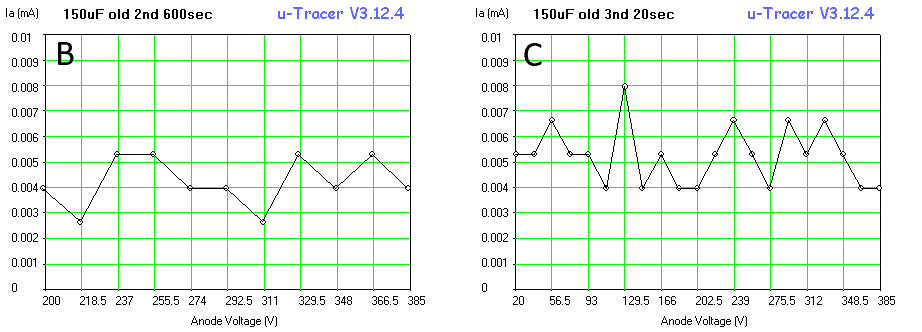
Figure 13.6 Also this never used 150uF / 385V capacitor from the Philips blue series shows low leakages current which slighty increases for higher voltages.
However, one formation cycle decreased the leakage currents to practically zero.
Links
On the internet many link to sites discussing capacitor formation can be found. Below a small selection for your (and mine) convenience:
I regularly get questions from users for higher currents. This combined with the fact that there are now some 1300 uTracers out there operating quite safely with the 200 mA current limit, motivated me to review the present current limitation and do some tests to see if the present limit of 200 mA can be raised to accommodate higher current tubes.
Before I continue, I would like to stress that these notebook pages are just what they are: notebook pages. Readers are very welcome to take them as a guideline of their own experiments, but caution should be taken. A 100 uF capacitor charged to 420 V is fearsome thing! Fortunately, should something go terribly wrong, the damage is usually limited to a few defect (<1 euro) transistors in the high voltage switch.
A short tutorial
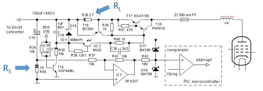
Figure 14.1 The standard uTracer3+ high voltage switch circuitry.
The maximum current the uTracer can source is mainly determined by the high voltage switches. Before continuing, it is a therefore a good idea to review how they work. In short a low power boost converter charges a 100uF reservoir capacitor (C18 in Fig. 14.1) to the desired voltage. During a measurement pulse, a high voltage switch with as main switching device the Darlington pair T17/T18 connects the reservoir capacitor to the anode (or screen) of the tube. The resulting anode or screen current also flows through current sense resistor Rs (R45). As a result of the direction of the current, this causes a negative voltage drop over Rs. OpAmp IC7 inverts this voltage because the AD converter on the PIC can only measure positive voltages. After the measurement the reservoir capacitor is discharged by closing T15 so that the energy is dissipated in R35.
A little complication in this simple scheme is that the entire high voltage switch has to be “floating.” What I mean is that the Darlington pair T17/T18 cannot be driven by any circuit connected to ground because in that case the current needed to drive the transistors would add up to the anode current and influence the measurement. The way this is solved is to isolate the high voltage switch from the rest of the circuit by means of an opto-coupler (OC2 in Fig. 14.1), while the energy needed to drive the switch is generated and stored locally in C19. The trick is that immediately before a measurement pulse, T15 is closed for 10 ms. This will charge C19 to 10V. The charge in C19 is enough to close the high voltage switch for 1 ms.
Another addition to the basic circuit is a hardware current limit. This simple circuit is implemented around R38 and T16. When the voltage drop over R38 exceeds ca. 0.7 V, T16 will start to conduct thereby drawing current away from the Darlington pair T17/T18. As a result, the current will not increase any further. Note that when the current limit kicks in, T17/T18 are no longer in saturation resulting in a voltage drop over the transistors. This is potentially a very dangerous situation since we have now both a voltage drop over the switch as well as high currents flowing, resulting in a high dissipation. This dangerous situation is detected by the software after which the PIC shuts down the switch automatically within 10 us.
So if we want to modify the current range we have in first approximation to consider the following points:
First experiments
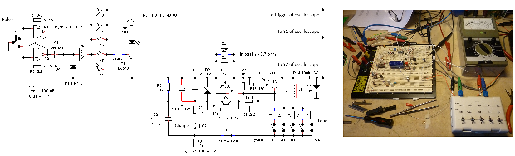
Figure 14.2 The test bench circuit used in the experiments.
Evaluating the high voltage switch in the uTracer circuit itself is not so simple. As mentioned, the high voltage switch is floating on the “high-side” of the circuit far above ground potential. This makes it difficult to do meaningful measurements in the switch circuit. For the experiments I therefore modified the test bench circuit that I also used for the original development of the circuit. In the test bench circuit, the entire high voltage circuit is brought to ground potential level making measurements straightforward.
Figure 14.2 shows the test bench circuit. It consists of a simple pulser that, when S1 is pressed, produces a 1 ms pulse in the LED of the opto coupler. Note that the entire high voltage switch circuit is now on ground potential level with the load connected to a variable negative potential. So when the high voltage switch is open, the output voltage is equal to the applied negative voltage. When the circuit is pulsed, the high voltage switch ideally brings the output to 0V. The voltage pulse resulting from the current through the current sense resistor (R6) is now positive with respect to ground. Since the whole thing is operated manually, C3 is now charged by briefly pressing S2 just before pressing S1.
The load of the high voltage switch is a set of resistors with switches that allows the output current to be set in steps of 50 mA from 50 mA to 1550 mA at the maximum output voltage of 400 V. The final thing that needs explaining is the function of R14 and D3. You have to imagine that when the HV switch is open, the output voltage can be as high (for the purists: at low) as -400V. However, what we are interested in is the small voltage drop over the HV switch when it is closed. To measure this voltage drop, the sensitivity of the Y-amplifier of the scope has to be set to something like 0.5V/div. However, when the switch is open, the high input voltage will drive the Y amplifier completely into saturation, resulting in all kind of artefacts which effect the measurement during the measurement pulse. The zener diode D3 prevents this by clipping the negative output voltage to -10V when the switch is open. Also have a look here.
Current limit
The maximum current that the high voltage switch can handle is in first instance determined by R9 that, with a value of 2.7 ohm, limits the current to approximately 250 mA. In the investigation into the limits of the current handling capability of the switch, R9 was lowered in steps by placing 2.7 ohm resistors in parallel to it, thereby extending the hardware current limit, in theory, by 250 mA for every resistor added. This is demonstrated in the left graph of Fig. 14.4 which was recorded using a modified uTracer with the compliance switched off.
The first thing noticed was that for currents in excess of approximately 500 mA the voltage drop over the switch started to increase during the measurement pulse (Fig. 14.3 left). If anything, I would have expected a decreasing voltage drop because during the measurement pulse the 100uF reservoir capacitor will discharge, resulting in a smaller current and hence a smaller voltage drop! After some searching it was found that with increasing current and hence decreasing gain of T2, the current drain on “local battery” C3 became so large that it could no longer feed the circuit. Adding an additional 10 uF capacitor parallel to C3 solved the problem (Fig. 14.3 middle). The value of 10 uF is somewhat of a compromise. It is large enough to ensure proper functioning of the high voltage switch even to 1A, while on the other hand it can still be fully charged to 10V by R7 during the 10ms “charging pulse” that precedes the measurement pulse.
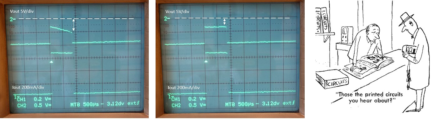
Figure 14.3 The graphs show the voltage drop over the HV switch (top trace) and the current through it (lower trace). The left graph is taken with C3 1 uF. In the right graph the 10 uF capacitor C4 has been added in parallel to C3.
The center graph of Fig 14.4 shows the measured voltage drop over the HV switch as a function of load current for different values of the current limiting resistor (R9 in Fig 14.2). Observe that for increasing current, the voltage drop over the switch steadily increases to 10V @ 1A. This voltage drop can be almost entirely attributed to the collector-emitter saturation voltage as indicated by Fig 3 of the datasheet of the KSA1156. The voltage drop over the high voltage switch cannot be compensated for in the GUI and causes a slight non-linearity for current in excess of 700 mA, however, it is so small that I am pretty sure most people can live with it. Note by the way, that at 1A the discharging of the reservoir capacitor as well combined with the voltage drop of the current sense resistor is becoming noticeable, resulting in a lower effective anode voltage than the set point anode voltage.
Looking at the datasheet of the KSA1156 it can be seen that we are pushing the performance of the KSA1156 to its limits. Fortunately as we say in Holland “the soup is not eaten as hot as it is served.” I spent the first half of my career as a semiconductor technologist and I know from experience that manufacturers in their datasheets are to say at the least conservative in specifying their components to account for process variations. I am pretty sure that on almost every parameter we have a margin of at least 20%!
Figure 14.4 Left: hard current limit behaviour for different values of R9 (measured on an adapted uTracer with compliance off and voltage limited to 150V). Middle: voltage drop over the HV switch as function of current for different values of R9 (measured at 400V). Right: nonlinearity measurement. The load resistor has been selected so that at 400V output voltage the current equals 1A.
Short circuit behaviour>
An important question to answer is how the HV switch will hold under full short circuit conditions. So far we only tested if the switch could handle the current while the switch was fully open with only a few volts voltage drop over it and thus limited dissipation. During a short circuit the full voltage drops over the switch while at the same time the maximum current is flowing, resulting in a peak dissipation than can amount to V*I = 400*1 = 400 W!! Fortunately this condition doesn’t last very long. The “compliance” circuit quickly detects a short circuit and switches the current off in approximately 6 us (read more here). Nevertheless, we are pushing the KSA1156 to the limits of its Safe Operating Area (see Fig. 4 in the datasheet).
To test the short circuit performance, C1 in Fig. 14.2 was adapted to produce pulses ranging from 5 to 15 us. Figure 14.5 shows on the lower trace the measured current for three different pulse lengths. The voltage was set to 400V (in the graph clipped to 10V) while for R9 four 2.7 ohm resistors were connected in parallel, setting the hardware current limit to 1A. From the measurements it is clear that even for pulse lengths that are about three times as long as what will occur in reality the switch holds. Does that mean that the HV switch will hold under all possible conditions? No, unfortunately not. Experience with the uTracer has shown that always situations can occur that will destroy the output transistor(s). Most dangerous are aggressive oscillations that cause a completely unpredictable behaviour and at high currents and high voltages can damage the circuit. Fortunately, the damage is in almost all cases limited to a few cheap transistors.
Figure 14.5 The lower trace in the graphs shows the current through the HV voltage switch for a complete short circuit. The hard current limit resistor consisted of four 2.7 ohm resistors connected in parallel. The voltage was set to 400V. During the pulse the KSA1156 is dissipating 400W! Even for a pulse length of 5 us, which is three times as long as what would occur in the uTracer, the transistor does not break down.
Adaptions to the user interface
The hard current limiting circuit works independent of the user interface. So modifying R38 (Fig. 14.1) does not require any modification to the GUI. However, the GUI does need to know the value of the current sense resistor R45 (Fig. 14.1) because it is used to calculate the current and for the “compliance” software current limiter. Until now the value of the current sense resistors was hard coded into the GUI software. Starting from version 3.12.6 it has become possible to explicitly specify the value of the current sense resistors.
This is done in the calibration form where an additional field has been added where the anode and screen current sense resistor values can be specified for the 300V / 400V and 50V uTracer versions. In this way it is for example possible to prepare the anode supply for high currents, while the screen section is working in the normal 200 mA range. Note, that after every change in either the selected version or the values entered for the current sense resistors, the values need to be saved to the calibration file which need to be followed by a restart of the GUI to make the new values effective.
Figure 14.6 To increase the maximum current range a new field has been added to the calibration form where the values of the current sense resistors can be specified.
Conclusions
From the above it appears feasible to greatly extend the current range of the uTracer by adding a few capacitors and resistors! Although a current range of 1A appears doable, it pushes the HV switch to its limits. Extending the current range comes at a small price. Since we are using only a 10 bit ADC to measure the currents, extending the current range to for example 1A reduces the resolution from 0.2 mA/bit to 1 mA/bit. If you are considering modifying your uTracer for higher current on a permanent base, I would recommend modifying it to 600 mA. In this range we are not pushing the circuit to its limits, while we still have a linear behaviour and an reasonable current resolution. I can understand that not everybody has the time or the patience to dive into the experiments described above, in the next section I will therefore describe a simple step by step procedure to convert your uTracer into a 600 mA version.
1. Starting point
For this write-up I assume that you have a working uTracer3+ (400V version) with the GUI 3.11 installed. In this step-by-step explanation I will show pictures from my own uTracer which happens to have the extra boost converter inductors. This is not essential at all; the same instructions apply to the standard uTracer configuration.
2. Stuff that you need
There is actually very little stuff you need for the conversion to higher currents. Nevertheless, if there is enough interest I will consider making a cheap “conversion kit.” Let me know!
You need:
3. Adding the capacitors
The capacitance of the 1uF capacitors C14 & C19 in the high voltage switches is increased by placing a 10 uF capacitor in parallel to them.
Fig. 15.1 shows how these capacitors can be added to the bottom side of the PCB. Please note the correct polarity of the capacitors.
Figure 15.1 10 uF capacitors added in parallel to C14 & C19.
4. Adjusting the value of the current limit resistors
The “hard-current limit” is set with R24 & R38. With the standard value of 2.7 ohm, the limit is approximately 250 mA. The current limit scales inversely proportional with the resistance. By adding per resistor another two 2.7 ohm resistors in parallel, the hard current limit is thus increased to 750 mA. Fig. 15.2 shows how these resistors rea added to the bottom side of the PCB.
Figure 15.2 Two 2.7 ohm resistors added in parallel per resistors to the current limit resistors R24 & R38.
5. Adjusting the value of the current sense resistors
The anode and cathode currents are measured by the voltage drop over the current sense resistors R20 & R45. The standard value of the current sense resistors has been chosen such that at the maximum nominal current of 200 mA, the voltage drop over the resistor (18*0.2 = 3.6V) is well within the range of the AD converter and still allows for some “overdrive.” By adding per current sense resistor two 18 ohm resistors in parallel, the nominal current range is tripled to 600 mA. Fig. 15.3 shows how these resistors are added to the bottom side of the PCB.
Figure 15.3 Two 18 ohm resistors added per resistor in parallel to the current limit resistors R20 & R45.
6. Check Modification
Use the pictures below to check the placement of the components.
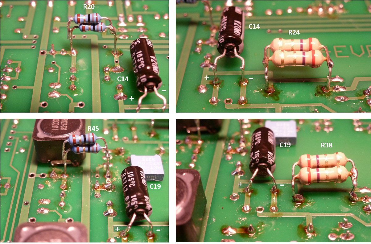
Figure 15.4 Placement of the components on the bottom side allows them to be easily changed without any de-soldering.
7. Download and install the latest version of the GUI.
Before you install a new version of the GUI, it is always a good practice to note down the current calibration values. So start-up your current GUI, open the calibration form and note down the calibration values. Then go to the beta version download page and follow the directions there to install the latest version (GUI 3.12.6 or newer).
After installation, start the new GUI and make sure it has imported the old calibration values. If it hasn’t done so for one reason or the other, then set the calibration values to their proper values and press “save”
Some people have reported that after they have installed and started the new GUI version the get a “Run time error; read beyond end of file.” When this happens you have to manually delete the old calibration files. If you restart the GUI after this, it will create a new calibration file and you will have to re-enter the calibration values by hand.
8. Enter the value of the current sense resistors into the GUI.
Open the calibration form on the newly installed GUI. For both the anode as well as the screen section we now have an equivalent current sense resistor of 18//18//18 = 18/3 = 6 ohm. Enter this value in the appropriate fields (Fig. 15.5). Then press “Save to Calibration File.” Then quit the GUI and restart the GUI to activate the new values.

Figure 15.5 Tell the GUI what the values of the current sense resistors are.
9. Calibration
Although the current sense resistors have a low tolerance, you may want to check and if an adjustment of the calibration is needed. To do so you can connect a 1k resistor between the anode (or screen) terminal and the cathode terminal. At a voltage of 400V check if the current measured is 400/1000 = 0.4A. If needed adjust Ia and Is gain sliders.
10. Ready to go!
You are now ready to go! You will note that now also the values in the “Range” and “Compliance” drop down menus have been updated. I would make it a good practice to set the compliance in normal use to a reasonable value of say 200 mA. Note that although I believe from the experiments described in the previous section your uTracer can handle the increased current range, it still has to prove itself “in the field,” so I am very much interested in your experiences.
Notes
Examples
Figure 15.5 The famous EL34 (6CA7) measured at full currents.
Figure 15.6 The PL519 (40KG6A) is a line driver tube used in the last generation tube colour televisions. Even 1A is not enough to fully characterize this beast!
Unfortunately, it is not possible to extend the grid bias range by simply modifying a few component values. One of the problems is that for a -100V grid bias you need, considering the fact that the cathode potential is 20V above ground potential, a -80V power source. That is with the present negative power supply voltage circuit impossible. After due deliberation I came up with two circuits. The first circuit uses a single high voltage OpAmp, but requires an external -85V power supply. The second circuit is fully self-contained, and generates its own -85V power supply, but unfortunately requires a new PIC processor. Both circuits work independent from the original grid bias circuit, which means that you can use both the original circuit and the new circuit in parallel.
Figure 16.1 The differential circuit (A) is most times used with R1=R2 & R3=R4 (B),
however, there is a third configuration where R1=R4 & R3=R2 that is also interesting and that is being used in the extended grid bias circuit (C).
Basic circuit
Before explaining the “extended grid bias circuit,” it is good to recall for a moment how the standard grid bias circuit in the uTracer works. As digital to analog converter one of the pulse width modulated (PWM) outputs of the PIC is used. This output produces a 19.1 kHz square wave with a duty cycle that can be varied between 0% and 100% with a 10 bits resolution. 0% Corresponds to a grid bias of 0V, 100% corresponds to -50V. The square wave signal is low pass filtered by IC4 (Fig. 16.2) so that at the output of IC4 a DC signal is obtained that varies with the duty cycle between 0 (0%) and 5V (100%). A complicating factor is that the cathode of the tube-under-test is connected (via diode D4) to the power supply of the uTracer, so ca. 20V. This means that the grid bias also needs to be referenced to this 20V. This is done with the circuit around IC3, T6, T7, which is basically a variant of the circuit depicted in Fig. 16.1C with the gain set to 10.
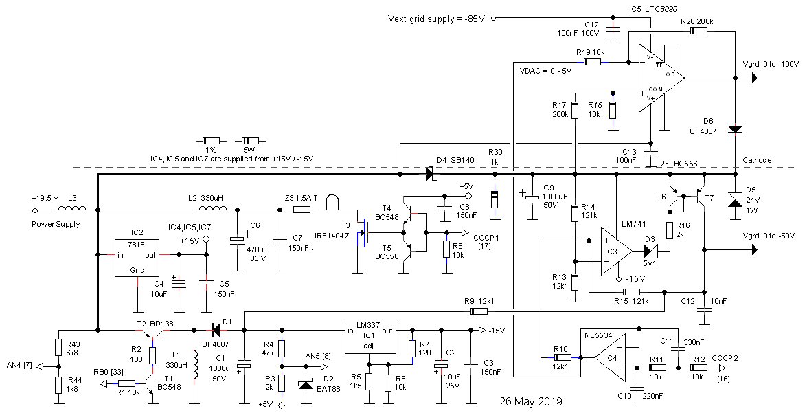
Figure 16.2 The basic variant of the extended grid bias circuit above the dashed line. The original uTracer circuit is shown below the dashed line.
Figure 16.2 shows the circuit diagram of the basic version of the extended grid bias circuit. The complete circuit consists of a single high-voltage OpAmp that is used in the configuration of Fig. 16.1 with the gain set to 20. The OpAmp used here is the LTC6090, one of the few affordable high-voltage OpAmps on the market. The LTC6090 can handle a total differential supply voltage of 140V with an (almost) rail-to-rail output voltage range and unit gain stability. Its only disadvantage is that it only comes in a SO8 SMD package with a thermal pad (more about that later).
The positive supply voltage of the LTC6090 is taken directly from the positive supply voltage of the uTracer, so approximately 20V. To obtain a 100V output voltage range, the negative supply voltage of the LTC6090 has to be at least -80V, preferably with a bit of margin, so -85V. It is possible to generate this -85V on-board, but it requires a hand full additional components and a new processor (see next section). However, if you have a (lab)-power supply at hand that can supply -85V, or if you are handy enough to construct a simple -85V supply yourself (the current consumption is only 1 mA), you can use the basic circuit shown in Fig. 16.2.
From the datasheet of the LTC6090 we learn that although the datasheet claims rail-to-rail operation, the maximum output voltage swing is limited to the positive supply voltage of the OpAmp minus 140 mV maximum at 1mA output current. Fortunately, we have this extra headroom as a result of Schottky diode D4, which introduces a voltage drop of at least 200 mV ensured by the current through R30. In other words, in contrast to the original grid bias supply, the output of the extended grid bias can really reach 0V.
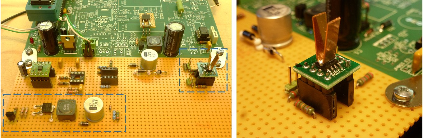
Figure 16.3 The extended grid bias circuit built on perf board being tested. The additional -85V power supply and the high voltage OpAmp are indicated by the dashed boxes.
Deluxe circuit
If you regularly need to test tubes that require the extended grid supply, then you probably want to integrate the -85V supply with the uTracer. Adding a -85V supply to the circuit is not so complicated, but it does require a new PIC. In the 16F874A used in the standard uTracer all 8 AD channels are already in use. The 16F884, which is a new and extended version of the 16F874A, houses in addition to the 8 ADCs already present an additional 6 ADC channels. Apart from this, I need to migrating from the 16F874A to the 16F884 anyway because the 16F874A will be phased out of production, and in anticipation of that is becoming increasingly expensive.
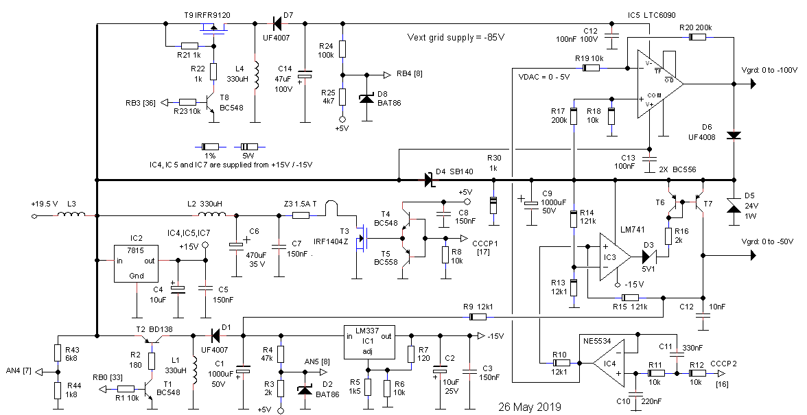
Figure 16.4 The extended grid bias circuit including the “on-board’ negative power supply is shown above the dashed line. The original uTracer circuit is shown below the dashed line.
Figure 16.4 shows the -100V grid bias circuit including the negative “high” voltage supply. The additional circuit is nothing more than a simple inverting boost converter, very similar to uTracer’s standard -40V supply. Like the other boost converters in the uTracer it is also controlled by the PIC. The firmware that controls the boost converters has been designed such that it can control at maximum eight boost converters at the same time (read here, here, and here). A big advantage is that the PIC can shutdown all the boost converters during the actual measurement pulse to reduce noise in the system. Instead of the BD138 I used a IRFR9120 PMOS transistor. The IRFR9120 is a readily available, very cheap 100V PMOS MOSFET and actually if there ever will be a new uTracer version, I think I will replace the bipolar BD138 with this more suitable equivalent.
As mentioned, the 16F874A PIC processer is gradually being phased out of production. The 16F884 is a more modern replacement with a lot of additional features. Because of the additional features some modifications to the PIC software were necessary. Despite the very useful tips Microchip published in a migration note, it still took me days of debugging to get the new PIC working flawlessly. The problem was in the routine that sets the PWM for the heater. Whereas in the CCP1CON register in the 16F874A bits 4 and 5 have not been implemented, in the 16F884 they control some of the new features of that module. Normally that would not have been a problem, but unfortunately during the setting of the PWM value, sometimes during a shift operation one of these bits got set. As a result an output pin that controls the PGAs got assigned another function. The end result were sudden and unpredictable bumps in the measured current. Anyway, I am just writing this down for myself so that I remember next time what the problem was.
No new GUI ……
For the moment I decided not modify the GUI for the extended grid circuit. When you want to use it, you have to remember that all values that you enter for the grid voltage are in reality a factor 2 higher. For example, the grid value series 0,-25,-50 will in reality correspond to 0,-50,-100. Please note also that in the quicktest, all derivatives towards the grid voltage like the transconductance (dIa/dVg) will be twice the real value. So you have to divide the measured values by two to find the real value! Should the extended grid bias circuit find a wide adoption, I will add the extended grid option to the GUI.
Finally
I am happy to supply a programmed PIC at minimum costs to people who want try the extended grid circuit! If there is enough enthusiasm for the circuit I can even consider making a small kit for it. Let me know by filling in the poll below. Multiple answers are possible.
That is not so easy. First of all, the maximum working voltage of electrolytic capacitors is fundamentally limited to around 450V. Secondly, boost converters are not really ideal for generating very high voltages. This is because the maximum voltage that can be applied over an inductor is limited, but more importantly, boostconverters require a switching transistor that has both a very low on-resistance as well as a very high working voltage, which are conflicting requirements.
More suitable are flyback converters. Flyback converters use a transformer to generate the high voltage. A very nice property of the flyback converter is that the switching transistor on the primary side “does not see” the high voltage on the secondary side, but only a voltage that is scaled down according to transformation ratio of the transformer. This makes the selection of the switching transistor much easier since on-resistance and output voltage now basically have been decoupled. If you want to know more about the basics of flyback converters have a look at a page that I wrote ages ago.
Unfortunately, flyback converters have one, for hobbyists, huge drawback: they require a transformer. Among hobbyists, including myself, transformers are not very popular. Either you have to make them yourself (…) or you have to rely on what is commercially available, which is usually not that much. However, some time ago I uncovered a cute little transformer that at first side might be perfectly suitable for experimenting with higher voltages for the uTracer. The transformer in question is manufactured by Würth with type number 750311486, and is available from Mouser with type number 710-750311692.
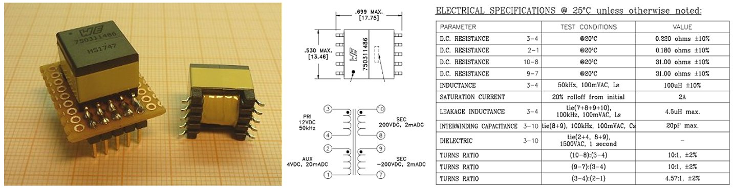
Figure 17.1 The 750311486 flyback transformer from Würth.
This little gem, which measures something less than a cube centimetre has four windings. A primary winding with an inductance of 80 uH, and two secondary windings, each with 10 times more windings than the primary winding. My idea was to use both secondary windings in series to generate voltages towards 1000V. Figure 17.2 shows a simple first test circuit to see if a flyback converter around this transformer would fit into the uTracer concept. The circuit consists of an oscillator that generates 10us wide pulses at a repetition frequency of 10kHz. On the secondary side, the two secondary windings feed two 100uF / 450V capacitors in series. A tricky pitfall of this circuit is the isolation between the two secondary windings. According to the specifications, the isolation between the primary and secondary windings is specified at 1500V. However, this is the isolation between primary side and secondary side. It says nothing about the isolation between the two secondary windings. To make it for the transformer as easy as possible, I made an elaborate construction with D1 … D4 that ensures there is no DC potential between the two secondary windings. Only during the flyback phase, there is a very short moment when all diodes are conducting, and where there can be up to 900V between the two windings.
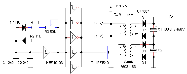
Figure 17.2 Circuit used to test the 750311486 flyback transformer from Würth under conditions resembling the uTracer topology.
The circuit worked like a dream. In less than six seconds, the circuit charged the capacitors to 900V! There was no sign of dielectric breakdown between the secondary windings. Note that at the primary side a simple IRFI540 transistor was used that is specified at 77mohm on resistance with a breakdown voltage of only 100V.
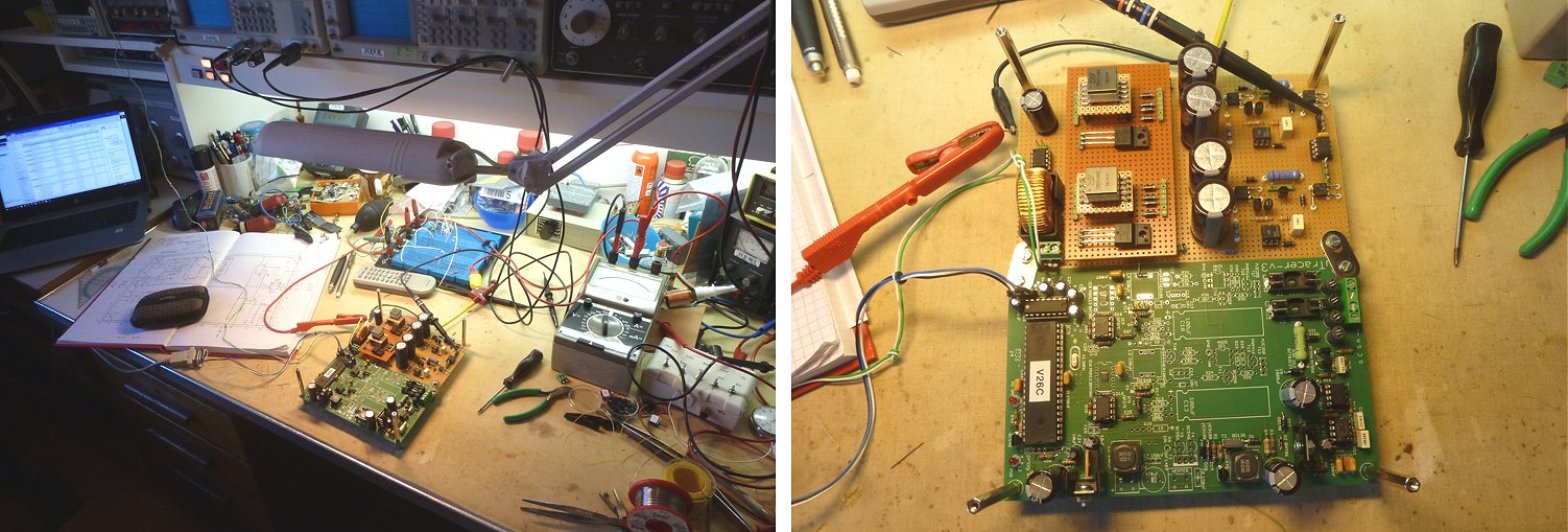
Figure 17.3 Full blown test circuit that I use(d) to study circuit concepts to increase the working voltage of the uTracer. On the perfboard there is a second “piggyback” perfboard that allows me to test different inductor/transformer configurations (Januari 2019).
The next step was to try the flyback transformer in an actual uTracer setup. Figure 17.3 shows a hacked uTracer where the high voltage section has been replaced by a breadboard implementation. The breadboard contains the high voltage section in a flexible and reconfigurable configuration, and a new high voltage switch (more about that in a future write-up). Because I don’t want to completely change the uTracer’s firmware, the flyback converter is driven in the same way as the standard uTracer, so with pulses of a variable length (0 to 50us) with a repetition frequency of 10kHz. The uTracer measures the voltage and stops pulsing when the voltage reaches the set point value. To my surprize and disappointment the circuit worked less well than I expected. The curves were raged, especially for voltages below 150V. Considerable time was spent on debugging the circuit. At first I suspected the oscillations that are common to flyback converters and that are caused by the charge stored on the drain of the MOSFET that cause oscillations after the transformer has delivered its charge to the load capacitor. Adding snubbers and diodes did give some improvement, but the circuit still continued to perform unsatisfactory.
I sometimes have the bad habit to start experimenting straight away without thinking too much or making calculations/simulations first. I plead guilty! After the initial disappointment I made some basic calculations that gave some clues as to why things didn’t work as expected. The most basic equation for any boost or flyback converter is given in Fig. 17.4A. It gives the current in an inductor with inductance L when it is applied to a voltage source Vsupl for t seconds. It basically says, when an inductance is connected to a voltage source, the current through the inductor increases linearly with time and at a rate inversely proportional to the inductance. Let’s take the flyback transformer as an example (Fig. 17.4B). If we apply 20V during 15us to the 100uH primary winding, the current in the primary winding will rise to 2A, the maximum current before the core starts to saturate.
Figure 17.4 Basic equation(s) governing working of a flyback converter.
When T1 is opened, the magnetic energy stored in the transformer will be dumped in the capacitor. The initial current flowing in the secondary side simply follows from the fact that the energy initially stored on the primary side of the transformer, is now transferred to the secondary side (Fig. 17.4D). So with a ratio in turns of a factor 10, the initial current on the secondary side is 2*sqrt(0.1)= 0.63A. Here we see one of the reasons why the circuit is not working as expected. The secondary current causes a large voltage drop over the secondary winding amounting to 0.63*62= 39V! This not only interferes with the proper flyback operation at low output voltages, but it also gives rise to substantial dissipation as could also be felt by the temperature of the transformer.
Back to the good old boost converter
After a lot of playing and tweaking of the flyback circuit, some improvement in the performance of the circuit was obtained, but it was too much of a hassle; the elegance of the circuit was lost.
Playing with the flyback converter, I realized however, that also in the boost converter concept the problem of a too high voltage over a single inductor could be solved by using two inductors in series! From the uTracer3 we know that this type of inductors can easily handle 450V across their terminals. By placing two inductors with half the inductance value in series, the current will flow through both inductors and consequently the generated voltage, which is proportional to dI/dt, will by definition be equally divided over the two inductors, potentially boosting the voltage up to 900V
Anode and screen voltages up to 900V would be great of course, but the problem of a switching transistor that can handle 1000V with a sufficiently low on-resistance and acceptable price and availability remained a problem. Fortunately it appeared that since the uTracer3 the industry has made significant progress. Silicon Carbide transistors with incredible specifications have now become available at very acceptable prices. An example is the SCT2750NY from ROHM that is available from Mouser under part number
755-SCT2750NYTB. This 1x1cm “monster” has a breakdown voltage of 1700V, and an on-resistance of only 0.750hm. It can handle currents up to 6A, a power dissipation of 57W, and comes at a price of around 6 euros. Apart from its large TO-268-2L package, the only other drawback that I can think of is that for the device to handle substantial currents, a gate voltage of around 15V is required.
Figure 17.5 900V Boost converter module.
Figure 17.5 shows the basic circuit of the high voltage boost converter. The circuit is pretty straightforward. The gate of the SiC fet is driven by a dual gate driver circuit. I used an IR25600, but many other gate driver ICs (like the MIC4427) will do just as well. The 8 pin package contains two driver circuits so that one can be used for the anode section and the other for the screen section. Resistor R1 limits the gate current during switching to a safe value. The filter consisting of L1 and C1 smooths out the high current boost pulses, which helps to reduce noise in the system. Finally, the two 2.7M resistors R2 and R3 ensure that the output voltage is equally divided over C3 and C4 even when is a small difference in leakage current in these capacitors.
Figure 17.6 To the left the modular test uTracer now with the boost converter installed. Note the large size of the SiC transistor! The picture on the right is just a small souvenir for myself of the holiday spent in Friensland in the North of Holland where we visited Foudgum, a tiny village in the North of Holland where the Dutch writer and poet Piet Paaltjens lived (summer 2019).
Figure 17.6 shows the same test board as in Fig. 17.3, but now equipped with the boost converter. The circuit worked like a dream, without any hitches! Note the enormous size of the SiC SCT2750 in comparison to the inductors! An added benefit of the circuit is that the saturation current of the 150uH inductors is much higher than the 330uH inductors in the uTracer3: 3A vs 1.5A. By simply increasing the length of the boost converter pulses to 35us, this current is reached. Since the energy stored in an inductor is proportional to the current squared, this means that per boost converter cycle 4 times the amount of energy (charge) is transferred to the capacitor(s). In plain English, they charge much faster, especially for voltages in the lower range.
Generating the required high voltages is of course only one part of the story of a higher voltage uTracer. We also need a high voltage switch that can handle 900V, or with a safety margin 1000V, and that can operate in a floating mode. The uTracer3 uses a simple PNP switch. As it turns out, it is very difficult to find affordable PNP or PMOS devices for such high voltages. However, NPN and NMOS devices for these voltages are readily available. In general N-type devices require a more complex driver circuit because the gate voltage has to be controlled with respect to the source that is floating. The gate voltage even has to become higher than the high side voltage rail when the device is fully on! As it turns out, for this application, also the P-type solution would require a special driver scheme to galvanically isolate the high voltage switch from the rest of the circuit, so in complexity there is not much difference. Having decided for an N-type device we still have to make the choice between an NPN bipolar transistor or an N-Channel MOSFET. Given the fact that for the MOSFET we don’t have to bother with a static gate current and that suitable high-voltage NMOS transistors are relatively cheap, the choice was easy. At first sight suitable transistors are the FQD2N100 from Fairchild or the STD2NK100Z from ST Microelectronics. These transistors have an on resistance of resp. 9 and 6 ohm, more or less independent of the drain current, so that it is quite straightforward to compensate for the voltage drop over the transistor after the measurement.
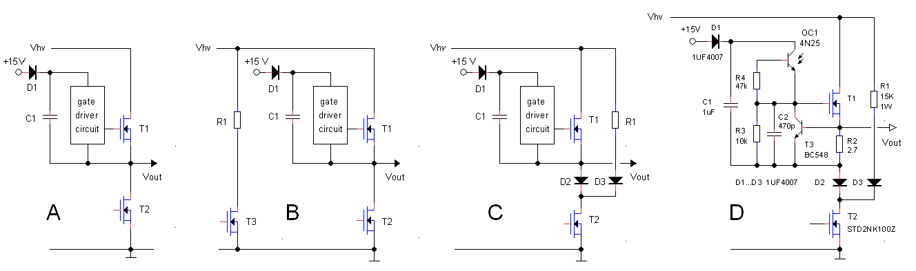
Figure 18.0
Just like in the uTracer3, the gate driver circuit is powered from a capacitor that is charged immediately before the measurement pulse. Figure 18.0A schematically shows the idea. Before each measurement pulse T2 is briefly closed, which charges C1 to 15V. Next T2 opens again leaving the high voltage switch circuit completely floating and only connected to the high-voltage source.
We should almost forget that also a means to discharge the capacitors needs to be implemented to discharge the capacitors when e.g. a new curve is measured of when the measurement is finished. The simplest way to implement this is to use a simple discharge resistor and tranistor in the same way as this is done in the uTracer3 (Fig. 18.0B) However, it seems rather a waste to use an additional transistor for that while we have another high voltage switch in almost the same “position” doing nothing most of the time: transistor T1 only needs to be closed a few milliseconds just before a measurement pulse! With a simple “OR” circuit consisting of diodes D2 and D3 we can have T2 perform the two tasks of discharging the reservoir capacitors and the grounding of high side driver circuit to charge the boots-trap capacitor.
Figure 18.0D shows a first attempt to an implementation of the high side gate driver circuit: R3 keeps T1 open when the transistor in the
opto-coupler is off. Transistor T3 and R2 form a simple current limiting circuit that is also used in the uTracer3, while C2 suppresses potential oscillations.
In the remainder of this section the high voltage switch will be analysed and tested to find out its operating limits.
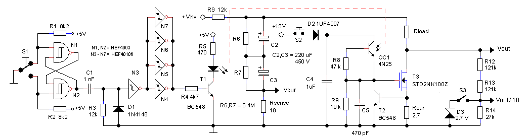
Figure 18.1 Test circuit for the NMOS high voltage switch
Analzing and testing an “high-side” circuit like the high voltage switch is not that easy. All the components are at a high potential with respect to ground and complicated differential probes have to be used to measure e.g. the gate-source voltage of the switching transistor. Fortunately, since the control input of the switch is basically isolated from the rest of the circuit through the use of an opto-coupler (the bias diode D2 Fig. 18.1 is normally off), it is possible to exchange the position of the load and the switch with respect to ground so that the circuit can be tested using ground as a reference.
Figure 18.1 shows the test circuit used in this section. Going from left to right we first find a pulse generator which simulates the measurement pulse normally issues by the PIC. It consists of a de-bounce circuit around N1 and N2, the pulse generator consisting of C1, R3, D1 and N3, and a buffer that eventually drives the LED in the opto coupler consisting of N4-N7 and T1. The pulse length is determined by C1 and R3.
A 150 nF capacitor results in a pulse length of approximately 1 ms, the normal measurement pulse length. A 1 nF capacitor generates a 10 us wide pulse which is approximately the pulse width when the processor interrupts the measurement because an over-load condition has been detected. The reservoir capacitor consists of two 220 uF / 450 V capacitors in series. Resistors R6 and R7 ensure that the high voltage is distributed evenly over both capacitors. The current is measured over Rsense, which causes a negative voltage drop over the resistor. The reservoir capacitor is charged via R9 by my (very) high voltage supply consisting of three stacked delta E0300-0.1-L 0 – 300 V power supplies, capable of generating 0 – 900 V. The voltage over the high voltage switch is measured with a 10:1 voltage divider (and a 10:1 scope probe). The zener diode is used for Ron measurements to prevent overloading of the scope input.
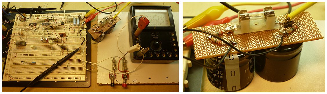
The operation in detail
The high voltage switch can operate in three different modes:
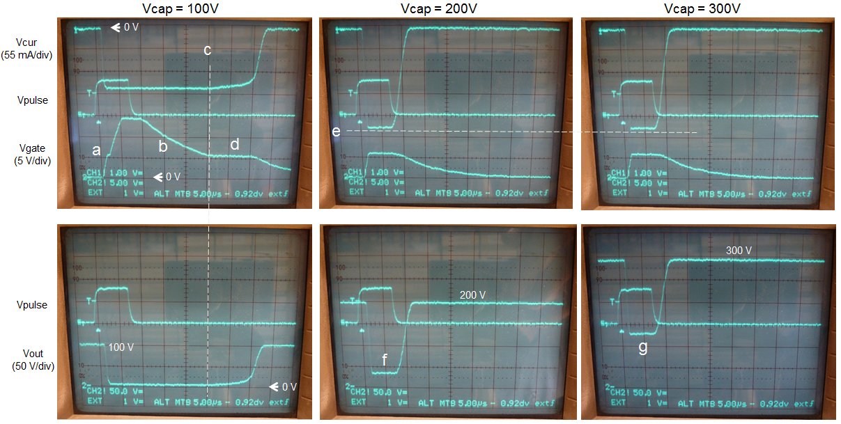
Figure 18.2 Analysis of the waveforms in the NMOS high voltage switch (see description below).
In Figure 18.2 the working of the switch in modes 2 and 3 is analyzed. For safety reasons the voltage is not pushed to the limit, but a maximum voltage of 300 V is used. The figure shows in three columns three different voltage setting: 100 V, 200 V and 300 V. The pictures in one column show different signals during the same measurement. The center trace in both pictures is the pulse signal that is also used to trigger the scope. In this case the pulse width is ca. 8 us. The upper trace in the top pictures shows Vcur which is the voltage drop over Rsense. The lower trace in the top pictures shows the gate voltage of the NMOS. The bottom trace in the lower picture shows the output voltage. Because the switch circuit has been shifted to ground level, the output voltage is high in the off-phase and should approach zero in the on-phase.
As load a resistor of 800 ohm is used. This means that with increasing voltage and the hardware current limit set at 250 mA (Rcur = 2.7 ohm), the hardware current limit protection will kick in at around V = R*I = 800*0.25 = 200 V. For 100 V the hardware current limit circuit is not yet activated. After the start of the measurement pulse, the photo transistor in the opto-coupler is switched on, and the gate voltage rises. The rise time is limited by the current the photo transistor can generate and the gate capacitance of the MOSFET. At Around 5 to 6 V gate voltage, the MOSFET switches on (Fig. 18.2a) and the output voltage drops. The sharp decrease of the anode voltage counter acts (through the drain-gate capacitance) the charging of the gate resulting in the kink in the gate voltage. Eventually the gate voltage rises to 15 V and the MOSFET is fully on. After the measurement pulse has been switched off, the gate is discharged by resistor R9 resulting in a logarithmic decay of the gate voltage (Fig. 18.2b). Since during that time the gate voltage is higher than the threshold voltage, the MOSFET remains fully on. At point c the gate voltage approaches the threshold voltage and the MOSFET starts being switched off causing an increase in anode voltage. The increasing drain voltage, again through the drain-gate capacitance, counter acts the discharging of the gate and actually stabilizes the gate voltage on a plateau value around the threshold voltage (Fig. 18.2d). At a certain point this balance situation can no longer be maintained and the MOSFET is finally switched off.
At 200 V the hardware current limit circuit has kicked in (Fig. 18.2 middle column). Note that the drain voltage in rest is 200 V, and but that during the measurement pulse the drain voltage is no longer zero but has increased to approximately 80 V (Fig. 18.2f). This is because the hardware current limit circuit has regulated the conduction of the MOSFET in such a way that it is now dropping these 80 V so that the current through the load remains constant at 250 mA. As a result the gate voltage is adjusted to a value slightly above the threshold. Since the gate voltages is already around the threshold voltage, and the drain voltage is no longer zero, the switch-off time is drastically reduced. For 300 V the current remains constant (Fig. 18.2e), which is only possible by allowing for a higher voltage drop over the MOSFET (Fig. 18.2g).
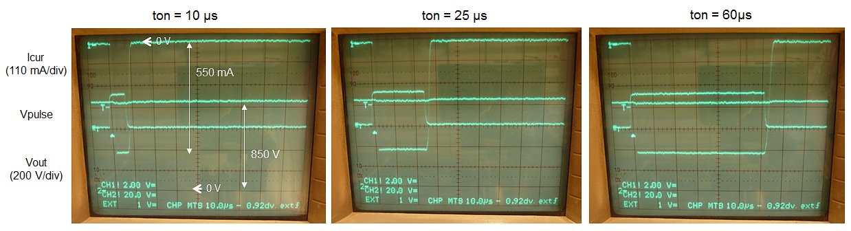
Figure 18.3 Switching characteristics at Vgate = 15 V (left column) and Vgate = 10 V (right column).
Figure 18.3 shows a similar set of curves as in Fig. 18.2 for a voltage of 100 V and a load resistor of 800 ohm (current limit circuit not activated). In the left column a gate voltage of 15 V is compared to a gate voltage of 10 V in the right column. By decreasing the gate voltages the discharging of the gate is significantly reduces (comp. a1 to a2 in Fig. 18.3) However, the plateau time remains the same (comp. b1 and b2). A gate voltage of 10 V seems optimal.
Pulse testing @ 550 mA
During the first tests it appeared that the NMOS high voltage switch easily passed all load and short circuit tests with the hardware current limit set to 250 mA. The hardware current limit was therefore set to 550 mA by lowering Rcur to 1.189 ohm (2.7//2.7//10).
Figure 18.4 Mode 1 testing at 550 mA (load = 1k5).
The first test was for normal operation with a measurement pulse length of 1 ms. Figure 18.4 shows the current as well as the drain voltage of the switch connected to a load resistor of 1k5. The load resistor was chosen such that the current limit circuit would just come into action between 750 and 850 V. The graphs show a perfect switching behavior even for the highest voltage and current combination.
Figure 18.5 Mode 2 & 3 testing around 550 mA (load 1k5)
In the second test Mode 2 and 3 operation is simulated with a mesurment pulse length of 10 us. A load of 1k5 is connected and the voltage is increased from 650 to 850 V (Fig. 18.5). At 650 V the hardware current limit circuit is not yet activated, the gate voltage of the MOSFET of 15 V, and the turn-off time is relatively long. At 750 V the current limit circuit is just activated and the pulse length is decreasing. At 850 V the current limit circuit is fully activated, the gate voltage is around the threshold and the turn-off time is minimal. The current is 550 mA.
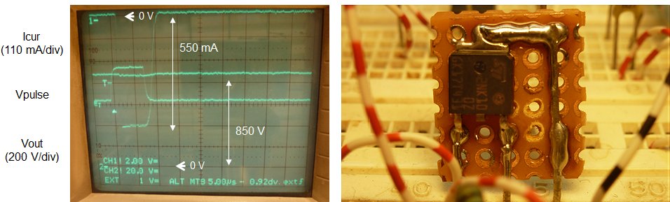
Figure 18.6 Full short circuit test at maximum voltage (850 V) and 550 mA! The tiny MOSFET in DPAK package is capable of handling an instantaneous dissipation of 425 W!
Finally a full short circuit test at maximum voltage (850 V)and maximum current (550 mA). Figure 18.6 shows how the tiny MOSFET handles an instantaneous dissipation of 425 W repeatedly without problems.

Figure 18.7 Exploring the safety margin
To investigate the safety margin we have with this switch circuit, the pulse length was increased in steps at maximum voltage (850 V) and full short circuit conditions (Fig. 18.7). It appeared that the pulse length could be increased to at least 60 us – 6 times the pulse length in reality – without problems. Most likely I could have gone further, but since this is evidence enough to convince me of the robustness of the circuit, and since I don’t like pushing buttons and waiting for a bang, I didn’t push it any further.
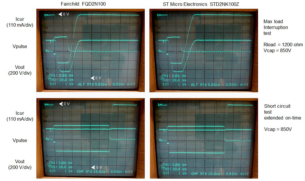
Figure 18.8 The FQD2N100 compared to the STD2NK100Z.
There are two 1000V MOSFETs that are readily available and reasonably priced: The FQD2N100 from Fairchild, and the STD2NK100Z from ST Micro Electronics. Their datasheets are pretty similar. The main difference is their price: the STD2NK100Z is about double the price of the FQD2N100. Under the assumption that more expensive also implies better performance all experiments so far were carried out using the STD2NK100Z. However, the comparison of the two in Fig. 18.8 shows that both transistors show almost identical behaviour and that FQD2N100 even shows slightly better turn-off characteristics.

Figure 18.9 Voltage drop over the MOSFETs as a function of drain current.
The voltage drop over a bipolar transistor in saturation is usually more-or-less independent of the current, and usually amounts to 100 to 200 mV. A MOSFET in the on-state in contrast behaves as a resistor with the on-resistance a function of the gate voltage. The voltage drop over the MOSFET will therefor depend on the current. This is not a problem, since – just as with the uTracer3 – the plotted current can be corrected for this voltage drop. To measure the on-resistance of the MOSFET, the voltage drop over the MOSFET (+ 2.7 ohm resistor) was measured for different currents taking care that the current limit circuit was not activated. To measure the Ron, the output voltage of the output voltage divider was limited to 2.7 V by means of zener diode D3 (Fig. 18.1). This allows for zooming into the low voltage drop when the MOSFET is on, while the input voltage is clipped when the MOSFET is off so that the amplifier of the oscilloscope is not saturated. The Ron (corrected for the 2.7 ohm resistor) has been plotted versus the current for both type MOSFETs in Fig. 18.9. The on-resistances for both types are indeed more or less constant and correspond well to the values specified in the datasheets.
Tackling dV/dt breakdown
While playing with the HV-switch test circuit (Fig. 18.1) a rather startling incident/accident occurred. I had the load resistor connected with two (isolated) clips, and at a certain moment I disconnected the load while the reservoir capacitor was charged to 900 V and T3 was not conducting. The moment I opened the clip, there was a big bang and the MOSFET, Rcur, Rsense, and a fuse I had in series with the capacitor were blown to pieces (Fig. 19.2)! What on earth had happened, and how can opening of a circuit result in such a violent event?
The most likely explanation is a dV/dt breakdown. Such a breakdown can occur when the rate of increase of the drain voltage exceeds a certain value. What happens is that the drain-gate capacitance causes a positive transient on the gate which not only momentarily opens the MOSFET, but which also may very well destroy the gate oxide causing the MOSFET to permanently fail. When I opened the clip I must have accidentally touched the lead resulting in a dV/dt breakdown.
One of the most effective measures to prevent dV/dt breakdown is to lower the impedance of the circuit that is driving the gate of the switching transistor. In the driver circuit shown in Fig. 18.1 the gate of the MOSFET in the off-state is connected to ground via a relatively high value 10k resistor. The lower the resistor value, the smaller the voltage spike on the gate. A simple push-pull buffer will drastically lower the impedance level and significantly reduce the sensitivity to dV/dt breakdown.
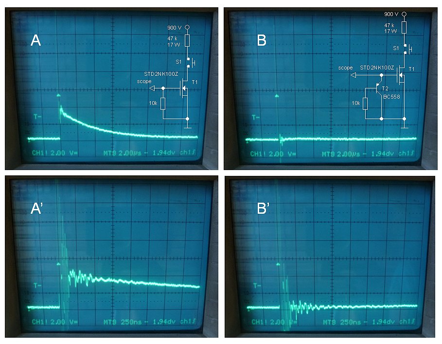
Figure 19.1 dV/dt testing without gate driver circuit (AA’) and with push-pull gate driver (BB’).
A simple experiment was used to get an qualitative idea of the impact of a buffer circuit on the dV/dt fenomenon. In Fig. 19.1A the drain of the MOSFET is connected via a push button and a current limiting resistor to a 900 V power supply. The signal on the gate of the MOSFET is monitored with a memory scope. When the switch is closed a transient appears om the gate. Figure 19.1A’ shows the same event on a different time scale. An extra transistor acting as an emitter follower almost completely suppresses the transient (Fig. 19.1B and B’). At t=0 there is in all cases a very large and very short spike that doesn’t decrease in amplitude when a buffer is used. I think is has nothing to do with the dV/dt effect but is just a measurement artifact.
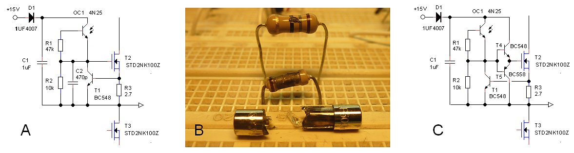
Figure 19.2 A) Original HV-switch circuit, B) collateral damage as a result of a dV/dt breakdown, C) new HV-switch circuit with gate driver.
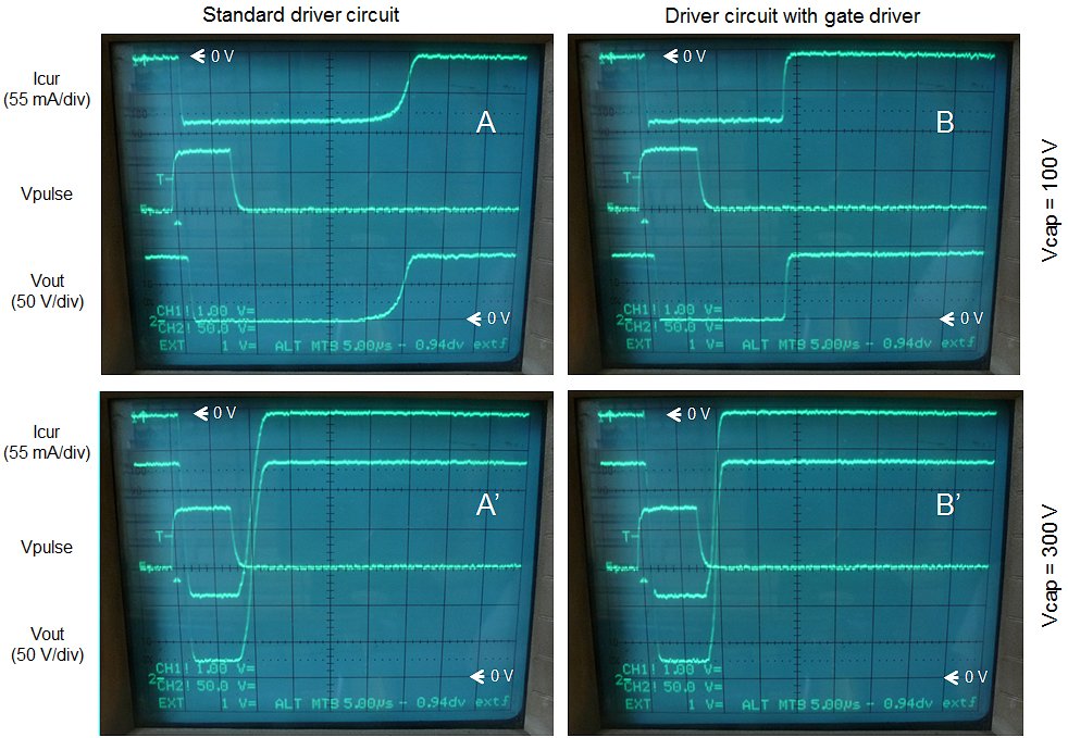
Figure 19.3 Switching behavior of the new HV-switch circuit compared to the standard circuit. Rload = 1 kohm
In the HV-switch circuit shown in Fig. 19.2C, a push-pull buffer circuit has been added to provide a low impedance drive circuit for the gate of the MOSFET. This does add some complexity to the circuit, but it greatly suppressed dV/dt related problems, while it also improves the switching speed of the circuit especially the turn-off time. This is illustrated in Figure 19.3. Here the switching behavior of the standard circuit (left two phortos) is compared to the circuit with the buffer stage (right two photos). In the top two photos the hardware current limit is not activated, while it is activated in the bottom two measurements. Especially in the case when the current limit is not active the reduction of the switch-off time is significant because the discharge of the gate-source capacitor is faster (Figure 18.3 part a1). However, the typical MOSFET turn-off behavior/time when the gate voltage passes through the Vt (Fig. 18.3 part b1) still remains.
Pulse testing @ 1 A!
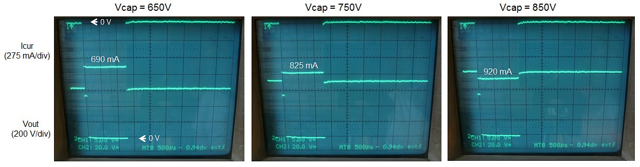
Figure 19.4 Standard 1 ms test. Rload = 900 ohm (1k//10k), Rsense = 2.7/4 = 0.65 ohm
During experiments with the HV-switch with the push-pull gate driver it was observed that the new circuit was much more stable in the current limiting regime. The 470 pF capacitor could be omitted without any problems and only for very low voltages oscillations were observed which readily disappeared for voltages higher than 100 V. It was therefore decided to again test the circuits up to currents of 1 Ampere! To set the hardware current limit to 1 A , Rsense was replaced by four 2.7 ohm resistors in parallel. Figure 19.4 shows the one millisecond Mode 1 test for voltages and currents around the maximum values. With a load resistor of 900 ohm and a voltage of 850 V, the circuit is tested at maximum voltage and maximum current. At the highest current the discharging of the reservoir capacitor is clearly visible
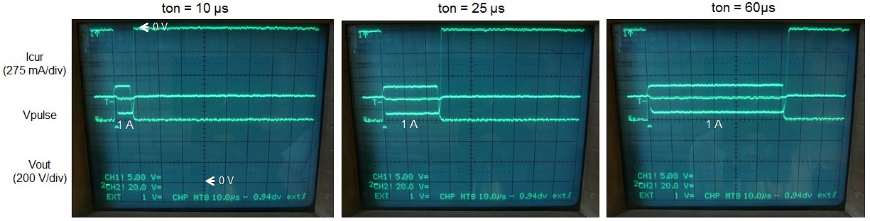
Figure 19.6 Full short circuit test extended times. Rsense = 2.7/4 = 0.65 ohm
Figure 19.5 Shows the high-speed switching behavior around the current limit region. The switching of 1 Amp at 900 V is no problem at all for the circuit. The switching speed is very fast, and the total on-time is very much determined by the control pulse width.
Finally, the robustness of the circuit was tested under full short circuit conditions at maximum voltage for extended times. The circuit easily managed to cope with repeated blasts at 60 us without problems!
Hi All,
Recently I was playing with ESP32 board (a rather cheap (5$) Arduino on 'steroids'), basically learning its possibilities and toying with it and I thought that it would be nice to have it connected to uTracer and make it act as a webserver on a local LAN (or even independently as a WiFi Access Point) and do all the measurements (and possible more) via web interface using a Mac or Linux laptop, ipad or mobile phone. After some attempts I put together such system, which is still highly experimental but it works good for my needs and I was wondering if someone would like to test it in the future or do something similar.
I do not have any manuals yet but most of the things are self-explanatory. Briefly, I am using ESP32 (a very advanced Arduino like board, for those who are not familiar with it), which runs a webserver, hosts all the webpages, and then uses its GPIOs to connect to uTracer and send AT commands, exactly as the standard Windows software for uTracer does. The software on the ESP32 consists of C++ code and Javascript. The ESP32 can be connected directly to Tx/Rx pins of the PIC controller (of uTracer), or in my case, I use a small adapter (Tx/Rx to RS232), so no changes to uTracer are necessary and the whole system is modular and can be connected via the RS232 interface (just needs 5V power).
Right now the system can:
I have some ideas for extra features, but most of them are based on what I typically do with the uTraces. It would be interesting to hear some ideas about possible additions, but it is a really hobby project, which is done over weekends (and not always).
I put all the webserver/javascript part of the code online and created a small website so anyone can upload their data and play a bit with the interface.
It is located at http://utracer.live There, the 'Acquire' part of course does not work, but all the visualization, modeling and load-line plotting are functional.
I made a few screencasts to show how things look in practice.
You can go to http://utracer.live and try yourself.
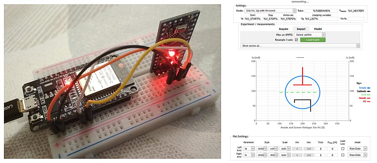
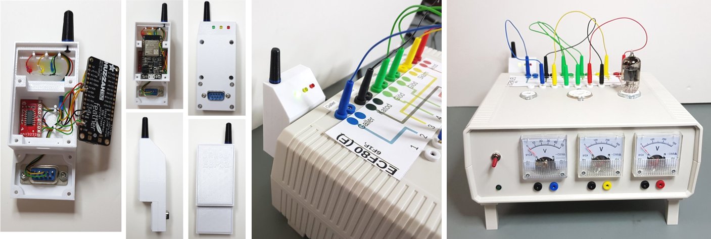
Have a look at the great ESP32 implementation by Tomas Lannestedt!
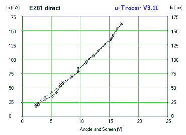 Recently a number of people have asked me how to measure or trace diodes or rectifiers with the uTracer. Since rectifiers are of course diodes, I will mainly use the term diode in this write-up. The problem with testing diodes with the uTracer is that by their nature the current through a diode increases very sharply as the voltage over the diode is increased, so that for most diodes already at 20 – 30 V the maximum current limit of the uTracer is reached. Unfortunately, as already discussed a number of times in these pages, the uTracer is not very good at accurately generating these (for radio tubes) very low anode voltages, especially not so at high currents. Let’s recapitulate why:
Add all this together and you and up with a “crappy” curve as shown on the right. Actually, you do not want to trace a diode by applying a voltage and then measuring a current that increases sharply with voltage. Ideally you would like to apply a current and then measure the corresponding voltage drop since the voltage drop increases only slowly with increasing current. In the end, you will of course end up with the same curve, but now in a much more controllable way. The simplest way to imitate this with the uTracer is to place a resistor in series with the anode!
Figure 21.1 shows the principle. The resistor has the same function as a series resistor for an LED. The resistor is selected in such a way that the voltage drop over the resistor is (much) larger than the voltage drop over the diode. In this way the resistor will to a large extend determine the current which is given by I = (Vu – Vd)/R, with Vu the voltage generated by the uTracer and Vd the voltage drop over the diode. Or, in other words, when the measurement is done, the voltage over the diode can be calculated from Vd = Vu – (I*R).
Figure 21.1 Left, principle of the diode / rectifier measurement with a resistor in series. Right, example of a single point current measurement on an EZ81.
A simple go / no-go test
I ques that most people who want to test a rectifier / diode are just interested if the diode can source the required current at a reasonable voltage drop. The simplest way to do that with the uTracer is to use a 1k resistor in series with the anode and then sweep the voltage to say 200V (Fig. 21.1 B). Without the diode this would result in a straight line all the way up to 200 mA. Since there is a voltage drop over the diode, the maximum voltage in reality will be approximately 30 V lower. Now what I do is, I place the cursor close to the 100 mA point (arrow 1). Then I read the corresponding voltage on the x-axis (arrow 2). Since at 100 mA the voltage drop over the resistor is 0.1 * 1k = 100V, I simply substract 100 V from that voltage, and that will give me the voltage drop over the diode. Most rectifier datasheets specify the 100 mA operation point and if not, you can read it from the curves.
I usually select the series resistor in such a way that I end up somewhere between 100 and 200 V. With a smaller value we again end up with the same problems as described above, but a larger value also compromises the accuracy. Everybody remembers from high school that is we substract two large numbers, a small inaccuracy can result in really big errors. That is also the case here. But of course you are free to experiment.
Diode curve tracing
Producing the I-V diode curve requires a bit more work. The way the curves in the examples below were produced is as follows: first a measurement with an appropriate series resistor is performed as described above. Next, the data is store in the Ia-list format. Next the data is imported in Excel and from the voltage and current columns the voltage drop over the diode is calculated according to Vd = Vu – (I*R). Finally, the measured current is plotted against the calculated diode current. In the examples below I have tried to scale the Excel plots in such a way that they can be directly compared to the graphs in the datasheets. I am not particularly an Excel wizard myself, but for those of you even less experienced in that miracle program, I have added a small video below.
Figure 21.2 A very common EZ81 (6CA4) double rectifier tube commonly used in radio’s etc. The left graph shows the uTracer measurement. The middle graph is taken from the datasheet. The recommended maximum operating DC current is between 100 and 180 mA. In this measurement a 500 ohm series resistor was used.
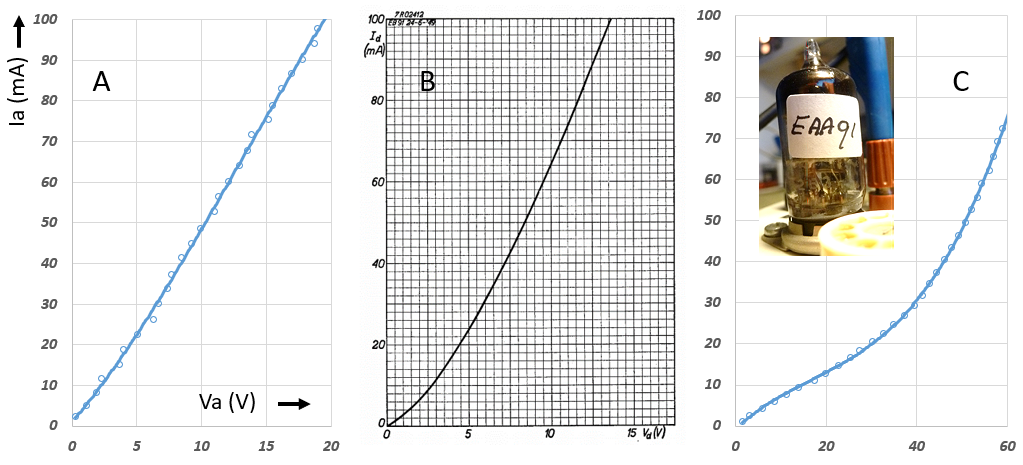
Figure 21.3 The EAA91 (6AL5) is a commonly used small signal double rectifier tube. The recommended operating current is 9 mA, although it can handle much higher currents. The figure on the left shows a good EAA91, the figure on the right shows a worn down version. In this measurement a 1K series resistor was used.
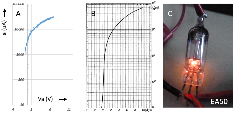
Figure 21.4 A rather exotic tube, the EA50 (6D1) using a 3k series resistor.
The tube was used as detector diode in RF equipment and in measurement equipment like the Philips GM6058.
This short video explains how you can import the measurement data into Excel to produce diode curves.
One of the nice things about the uTracer testimonial page is that I get a bit of an insight into the sort of tubes people want to trace. From the testimonials I received from people who built the uTracer6, I was astonished to see what “monster tubes” especially ham radio enthusiasts are using! Whereas I would have thought that the uTracer6 with its 1000 V and 1 A anode and screen supplies would cover all possible audio tubes, it appears that for most transmitter tubes the uTracer6 only covers a small part of their operation area. Not surprising, just like Dickens’ Oliver Twist, the proud owners of these tubes are asking “Please Sir, can I have some more!” I took it as a challenge to think about circuit concepts that will allow for full tracing of these monster tubes. It should be clear that, although I may do some experiments to test concepts, I have at this moment no plan whatsoever to make a uTracer kit for these very high scary voltages. Also because I do not want to be held liable should something go wrong!
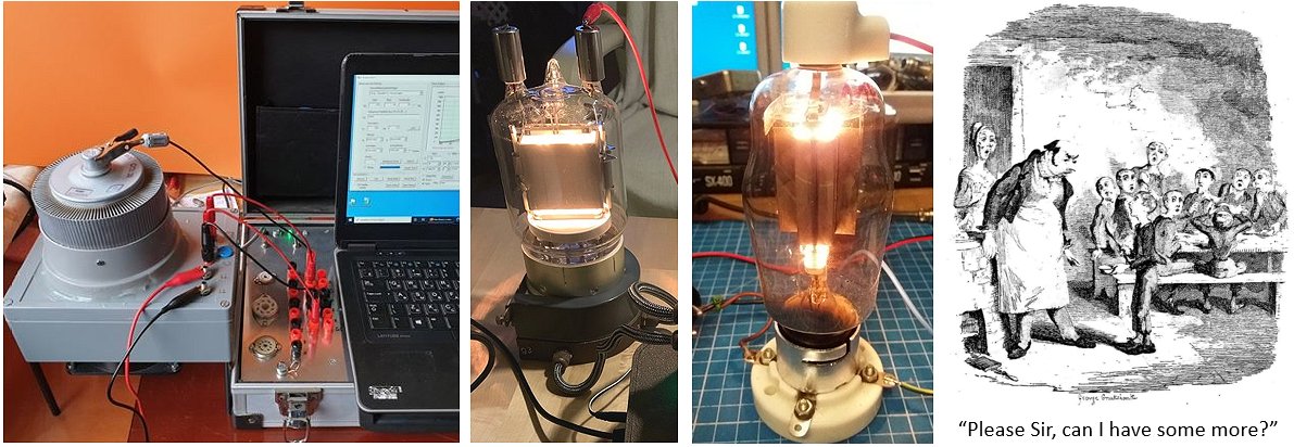
Figure 22.1 Some pictures from my testimonial page of the monster transmitter tubes being traced with the uTracer6.
Although with its 1000 V anode voltage the uTracer6 makes a good start, most people like Oliver Twist “would like to have some more”!
I made a small search on internet into the type of tubes ham radio amateurs use in their transmitter amplifiers. A small collection of them can be found in Fig. 22.2. It appears that anode voltages up to 5 kV at a current between 1 and 2 A would cover most tubes.
Figure 22.2 I made a small search on the internet into the type of tubes ham radio amateurs use in their transmitter amplifiers. It appears that anode voltages up to 5 kV at a current between 1 and 2 A would cover most tubes.
The Marx generator
My first idea was to revive the transformer idea again that I explored - and for various reasons abandoned - in the uTracer4 concept. The main attraction of that concept is its robustness. It appeared to be almost impossible to damage the circuit by a shorted output. Another attractive feature that I had in mind was to make the concept modular, so that to achieve higher currents more units could be placed in parallel. I looked at it with my colleague and transformer specialist Peter Bancken. We both agreed that that the concept could work, however, it would require a specially made transformer that had to combine a high output voltage with a very low spreading inductance, requirements that are difficult to combine.
Figure 22.3 Principle of the Marx impulse generator (left); giant Marx generators (right) can produce pulses of millions of Volts and are used, for example, to test components in electricity distribution networks.
The idea of making something modular, where either higher currents or voltages can be obtained by switching units in parallel or in series somehow reminded me of the giant Marx impulse generator we had at the high voltage lab of my university in Eindhoven. From Wiki: a Marx generator is an electrical circuit first described by Erwin Otto Marx in 1924. Its purpose is to generate a high-voltage pulse from a low-voltage DC supply. Marx generators are used in high-energy physics experiments, as well as to simulate the effects of lightning on power-line gear and aviation equipment.
A Marx generates a high-voltage pulse by charging a number of capacitors in parallel, and then suddenly connecting them in series. Figure 22.3 shows the basic circuit. First, n capacitors C are charged in parallel to a voltage Vhv by a DC power supply through the resistors R (Fig. 22.3A). The spark gaps are used as switches, and have the voltage Vhv across them, but the gaps have a breakdown voltage greater than Vhv, so they all behave as open circuits while the capacitors charge. To create the output pulse, the first spark gap is caused to break down (Fig. 23.3B); the breakdown effectively shorts the gap, placing the first two capacitors in series, applying a voltage of about 2*Vhv across the second spark gap. Consequently, the second gap breaks down to add the third capacitor to the "stack", and the process continues to sequentially break down all the gaps (Fig. 23.3C). With all capacitors in series, an output pulse of n*Vhv is obtained at the last stage. The charge available is limited to the charge on the capacitors, so the output is a brief pulse as the capacitors discharge through the load. At some point, the spark gaps stop conducting, and the voltage supply begins charging the capacitors again.
Searching for “Marx generator” in Google will return many hits of both professional as well as amateur builders of Marx generators, obviously with the sole purpose to produce giant sparks. I especially like the YouTube video from ElectroBOOM!
A Marx uTracer?
Figure 22.4 Schematical representation of the modular high voltage uTracer.
Since the uTracer also operates in a pulsed fashion, it seemed obvious to explore if the Marx concept can be adopted for a very high voltage uTracer. One very attractive aspect of the Marx generator is that during its operation both the resistors as well as the capacitors are never subjected to a voltage higher than the input voltage. This is very attractive since above 1500 V electronic components become very scarce and prohibitively expensive. A major difference with the standard Marx generator is that in the uTracer we need to interrupt the current after a fixed period of time of 1 ms, while in the Marx generator the current continues to run until the capacitors are so far discharged that the spark gaps open again. After some puzzling I came to a circuit that might do the trick.
The basic operation of the circuit is schematically explained in Fig. 22.4. At the center of the circuit in Fig. 22.4A we find capacitors C1 – C4, which obviously form the heart of the Marx generator. Note that on the bottom side of the ladder structure the resistors have been replaced by switches S1. On the top side of the ladder structure the resistors have been replaced by diodes. On the left side the ladder structure is not directly grounded, but connected to ground by a small series resistor that obviously will be used to measure the current during the measurement pulse. The DC voltage source in the traditional Marx generator has been replaced by a boost converter consisting of T1, L1 and D0. On the right side of the ladder switch S4 has been added to discharge the capacitors through Rd when needed. Finally, the spark gaps have been replaced by switches S2.
Operation:
(the letters refer to the corresponding figure in Fig. 22.4)
Towards a circuit
It will not come as a surprise that in the real circuit implementation that I have in mind the switches are replaced by transistors. The obvious challenge will be to find a simple way to control the transistors. Let’s first discuss voltages. To keep the total circuit as small as possible the voltage per ladder stage needs to be as high as possible. The SiC SCT2750NY transistors are rated at 1700 V, combined with an Rdson of 0.75 ohm and a continuous drain current of 6 A! For me they are the ideal candidate for all the high voltage transistors. To be on the safe side, the maximum voltage per ladder stage was set at 1500 V.
Figure 22.5 Simplified circuit diagram of the modular high voltage uTracer.
Figure 22.5 shows a simplified version of the actual circuit implementation. Going from left to right we first find the traditional booster configuration that is used in the other uTracers. To reach the 1500 V working voltage I plan to use three 330uF / 500V electrolytic capacitors in series. To ensure that the total voltage distributes evenly over the three capacitors, usually a resistive divider network is used. However, selecting the proper resistor values is tricky and besides this the resistors also dissipate. So here I plan to use Zener diodes that limit the voltage per capacitor to a value slightly above 500 V. When the voltage across a capacitor exceeds the maximum value the diode starts to conduct, forcing more current into the other caps.
Next, we move to the ladder sections. Transistors Ta obviously implement the switches S1 from Fig. 22.4. The gates of these transistors are controlled by a bus labelled “Open ladder.” This is an active-low signal. When it is 0 V, diodes Da block and the gates of the transistors are pulled low (with respect to their sources) by a resistor. When it rises to 20 V, first the most left transistor whose source is practically connected to ground via Rs will start to conduct. This will also pull the source of the second transistor Ta to ground so that also that transistor will turn on, etc. When the ladder is “erected,” and the different sections will be at a high potential, diodes Da will block, and the transistors Ta will be off. This means that some of the diodes Da will need to be able to block the maximum output voltage of the circuit! The high resistivity resistors Rl have been added to prevent the different branches of the ladder from “floating” when the transistors Ta are open.
When the ladder is in the “charging state,” the total equivalent high voltage capacitance for the circuit in Fig. 22.5 is: 3 x (330 uF / 3) = 330 uF. The first question now is: is it possible by using a simple boost converter, to charge a 330 uF capacitor to 1500 V in a reasonable time? I will come back to that question later. Apart from this, in the “erected state” all the capacitors are in series, and we end up with an equivalent capacitance of 330 uF / 9 = 37 uF. This is not so far off from the 50 uF in the uTracer6, but it is getting a bit on the small side. Up till now I have used the 10 ADC inputs of the microcontroller to sequentially poll the analog inputs. However, this inevitable means that there will be a time difference between the moment the voltage is measured and the moment the current is measured. In between these moments, the voltage of the capacitors may have dropped significantly. So for the first prototype I plan to use sample-and-holds, that capture both the voltage as well as the current at exactly the same moment.
The transistors Tb in Fig. 22.5 implement the switches S2 in Fig. 22.4. People who have studied the circuit diagram of the uTracer6 will undoubtably recognize the gate driver circuit for Tb. The circuit makes use of the fact that “bottom side” of the ladder will be at ground potential most of the time. In this state capacitor Cb will be charged to 20 V through diode Db. The capacitor acts as a little battery to power the gate driver circuit during the 1 ms measurement pulse. When transistors Tb are not conducting, their gates are tied to their sources by a resistor. The transistors are controlled by optocouplers that uses the charge stored in capacitors Cb. For the optocouplers I plan to use the affordable CNY66 that isolates voltages up to 13.5 kV.
On the right side of Fig. 22.5 we find the discharge circuit and the final output switch. In the discharge circuit transistor T2 fulfills two tasks. First, T2 is used to discharge capacitors Ca (if needed) through resistor Rd. At the same time T2 grounds capacitor Cb so that it can be charged. The output switch is identical to the ladder switches.
Figure 22.6 Detailed circuit diagram of the modular high voltage uTracer.
The open spaces in Fig. 22.5 already suggest that this is not the complete circuit. Correct! The way the gates of the transistors are driven in Fig. 22.5 is a bit too simple. The grid resistor that pulls the gate down unavoidably has a rather high impedance. Any fast transient on the drain can, through the drain-gate capacitance, pull the transistor into conduction with potentially disastrous consequences (read more about the so called dV/dt breakdown here). To tie the gates of the transistors firmly to ground when they should remain closed, totem pole buffers consisting of an emitter follower npn/pnp pair have been added. Actually, this small circuit is identical to the high-voltage switch driver already tested in the uTracer6.
Loose ends
Figure 22.7 Ta and Tb are protected by the Zener diodes across the electrolytic capacitors.
Although in principle the high voltage transistors in the circuit are never subjected to a voltage higher than the maximum voltage of a single ladder stage, it turned out that the Zener diodes used to guarantee the proper voltage distribution over the electrolytic capacitors also offer additional protection. When for example the voltage across Tb in Fig. 22.7a would become too high, the voltage is clamped by the stack of Zener diodes on the right side of the stage. Conversely, when the voltage across Ta becomes too high (Fig. 22.7b), the “body diode” of Tb opens and the voltage over Ta is clamped by the stack of Zener diodes over the capacitors on the left side of the circuit. The body diode is in circuit diagrams often omitted because in most circuits the drain always remains positive with respect to the source, however, here it is used to offer extra protection to the circuit. In the case of the SCT2750N the characteristics of the body diode are separately specified in the datasheet. It can handle a continuous current of 6 A and a peak current of 14 A.
Figure 22.8 Boost converter variations
It can easily be overlooked that also the inductor in the boost converter must be able to handle the full ladder stage voltage of 1500 V. From the extensive experience with the uTracer3 and 6 it is clear that the inductors from the DR127 series from Coiltronics / Eaton can perfectly handle voltages up to 500 V. By simply placing a number of inductors in series the maximum voltage can be distributed over the separate inductors. Since the induction voltage over the inductors is directly proportional to dI/dt, and since the same current flows through all the inductors, the voltage will always be evenly distributed. In the uTracer6 two inductors were used in series to be able to handle 1000 V. In this case three inductors of 100 uH can be used to roughly obtain the 330 uH to match the pulse length of the firmware controlled boost converters.
Mainly for my own administration a list of components I have in mind for the 5 kV uTracer:
While experimenting with the circuit of the 5 kV uTracer discussed in the previous section, something went wrong which left the high voltage reservoir capacitors partly charged. Fortunately, I thought of it, could discharge them safely, but had I forgotten to check them, I could have been in for a very nasty surprise! Not wanting to rely on my alertness to continuously check the status of the capacitors during experiments, I felt the need for a circuit that will warn me if the capacitors are charged to a dangerous voltage. It resulted in a simple circuit that might be of interest to other uTracer owners who want to add some safety to their uTracer builds.
Below the design requirements for the lifesaver:
Figure 23.1 The conception of the lifesaver step-by-step.
Obviously a circuit that makes a current of a few micro-amps flash an LED will need to consist of a capacitor and some form of threshold detector with switch that discharges the capacitor through the LED. The basic idea of the circuit is shown in Fig. 23.1A. It consists of two parts, a current source that limits the current drawn by the circuit to a few micro-amps and makes it independent of the input voltage, and the flasher circuit.
Let’s first concentrate on the flasher circuit. The simple idea was to let the current charge capacitor C1 until the voltage over the capacitor becomes so high that zenerdiode D1 starts to conduct thereby triggering thyristor D2. The thyristor discharges the capacitor through the LED until the capacitor is discharged, and the thyristor comes out of conduction. The low power thyristor can conveniently be implemented by a pnp transistor tightly coupled to an npn transistor Fig.23.1B (also have a look here). The problem with this circuit is that the gain of common transistors is so high that the smallest noise in the circuit will trigger the thyristor at unpredictable moments. The problem is easily solved by connecting two high value resistors over the emitter-base junctions of the two transistors Fig. 23.1C. This will effectively kill the gain of the transistors at low currents, making it a reliable simulated thyristor.
Disappointingly, the circuit still did’t work as expected. The capacitor charged as it should, and when the capacitor voltage increased beyond the voltage of the zener diode the thyristor fired as expected flashing the LED and at the same time discharging C1. However, instead of starting the cycle all over again, the circuit froze at the point where the current supplied to the circuit would just keep the thyristor conducting. The solution to this was to include a small inductor in series with the LED (see Fig. 23.1D). The inductor in combination with the capacitor forms a resonant circuit that gives the circuit a flywheel character whereby the current is really pushed to zero so that thyristor comes out of conduction.
The circuit of Fig. 23.1D worked well, but only for reasonable currents. For currents in the few micro-amp range the circuit again froze in a state where the current needed to trigger the thyristor was larger than the current supplied to the circuit. So for this circuit to work, the current drawn during the charging of the capacitor should be an order of magnitude or more less than the supply current. This was easily remedied by the addition of MOSFET T3 (Fig. 23.1E). With zenerdiode D1 in series with the gate, T3 will only start to conduct when the gate voltage exceeds its threshold voltage plus the zenerdiode voltage, while the gate of T3 of course draws zero current. Note that in this case the thyristor is not trigger by pulling the base of T2 up, but by pulling the base of T1 down. This really did the trick and the circuit now works very satisfactory even for currents well below 1 uA.
Before attentive readers start writing me emails, I know that there are special energy scavenging ICs like the LTC3588 or the S6AE101A, but that would have been half so much fun, and they are quite expensive anyway.
Figure 23.2 Left, connection of the lifesaver circuit to the uTracer in case each capacitor has its own lifesaver circuit. Right, connection if one circuit is used to monitor both capacitors.
What remains to be discussed is the current source. For that I used a circuit that most of you will recognize as the current limiting circuit in many simple power supplies. It consists of transistor Ta that is basically pulled into conduction by resistor Ra (topside of Fig. 23.1B). Rb senses the current and as soon as the current exceeds approximately 0.8 V, transistor Tb will start to conduct thereby cutting off Ta. This will stabilize the current at a value determined by Rb. I used a MOSFET for Ta since I didn’t want to bother with a base current and I had some lying around anyway. Diode Da protects the gate of the MOSFET against an excessive gate voltage should anything go wrong.
In Fig. 23.2 some component values have been added to the circuit. For the 1000 V version of the circuit an FQD2N100 or STD2NK100 or equivalent can be used for Ta. If you want to use the lifesaver for the uTracer3 obviously a transistor with a lower breakdown voltage can be selected. Resistor Ra should be as high as possible since the current through this resistor adds to the total current making the current source voltage dependent. I used a 500 Mohm resistor from Murata (available from Mouser). The MHR_SA series of resistors from Murata offers resistors up to 1 Gohm with up to 20 kV rating for a very reasonable price. For the inductor I used a 100 uH axial type, the value is not particularly critical. I don’t know where I got this particular inductor from, but I guess that any readily available inductor like this one available from Mouser will do. For the LED a high intensity type gives the best results. I used a 3500 mcd white VAOL-3GWY4 from VCC.
Figure 23.2 shows how the lifesaver can be connected to the uTracer. If you plan to use a seperate lifesaver circuit for each of the two high voltage electrolytic capacitors the circuit can be connected directly over each of the capacitors (Fig. 23.2A). In this way, the current used by the circuit is not flowing through the current sense resistor and so is not detected at all. It is also possible to use one circuit for both capacitors by using two diodes in an “or” configuration (Fig. 23.2B). Obviously, in that case it is unknown which of the two capacitors (or both) is charged.
The (rather poor) movie below shows the circuit in action on breadboard. I am not going to bother designing a PCB for it, but will simply transfer it to perfboard(s). It is fun to experiment with the circuit. Increasing the value of C1 will increase the intensity of the flash but reduce the flash frequency. This can be compensated for by increasing the current by lowering the value of Rb. The voltage at which the circuit starts flashing can be adjusted by changing the breakdown voltage of the zener diode, which will also effect the brightness of the flash etc etc. In the test setup shown in the movie below I connected a piezo speaker in parallel with the LED to also give an acoustic feedback signal. Perhaps a small normal speaker in series with the LED will also work and provide enough inductance so that L1 is not needed? In short, have fun but be careful with high voltages!
For uTracer Readers
Tube-Models is a web-based companion to uTracer: upload the `.utd` file, see clean curve plots, overlay classic tube models, and get SPICE-ready parameters—no installs required.
How It Compares
Similar to Derk Reefman’s ExtractModel, but fully browser-based and easier to use.
All math algorithms for parameter extraction are included, so you can fit triode, tetrode and pentode models directly from your uTracer data.
What You Get
Model fitting: Aligns theoretical curves to your measurements and extracts parameters like `mu`, `kp`, `kg1`, `kvb` for simulators.
SPICE testing: Provides ready-made SPICE circuit files to simulate your fitted model and compare against the original uTracer curves.
Curves and overlays: Visualize grid-voltage families vs plate voltage with model overlays to spot matches and deviations.
Sharing & Repository
Open by design: The code, uploaded measurements, and generated SPICE models are public.
Central library: The site supports sharing and browsing tubes and their models, acting as a community repository for uTracer measurements and SPICE parameter sets.
Why it’s Useful
Turn measurements into decisions: Export SPICE parameters and test circuits straight from your uTracer files.
Fast, friendly, shareable: Web UI; ideal for hobbyists and builders who value convenience and community.
Rogelio made a short movie, demonstrating the use of “Tube-Models.”
Click here if the movie above does not play correctly.
A short manual to using “Tube-Models”
| 1 |
Open the following URL in the browser (chrome or Edge recommended/tested) https://audio-projects.us/tube-models/ |
| 2 | Select an existing tube (e.g.: ECC85). |
| 3 | You will see on the right side the models that have been calculated for this tube, in case of a triode, only the Norman Koren Triode Model is available. |
| 4 |
To validate the model against the measured data from the uTracer, select one of the imported files in the center section.
|
| 5 |
Click on the "Plot file data icon"  The uTracer file will be displayed |
| 6 |
Select in the dropdown the calculated model (Norman Koren Triode Model). The model will be plotted (evaluating the equations) and presented on top of the measurements.
|
| 7 | Adding a new tube is similar to the procedure described above with the exception that the user needs to upload the uTracer files (.utd) and press on the button to calculate the model. |
The entire Tube-Models project is open source, and the repository is available here:
https://github.com/audio-projects/tube-models

Impressions from the Tube-Models parameter extraction tool.


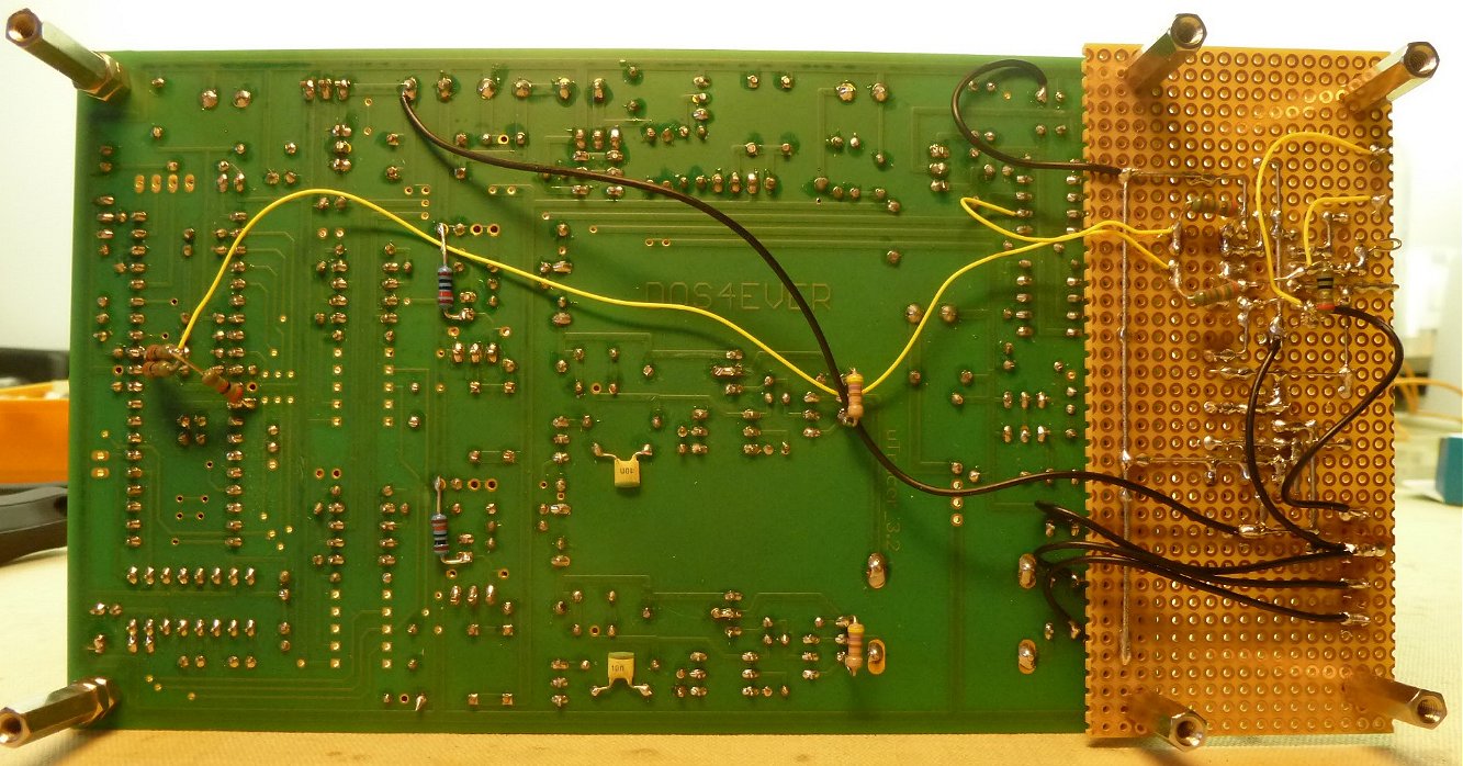