

|
|
|
|
Contents:
|
|
I think that I am not exaggerating when I write that the uTracer3 has been a great success. At the moment of writing of these lines some 500 uTracer3 kits have been sold all over the world, and as far as I can see all of them are working as expected. The uTracer3 was a compromise between simplicity and performance and was originally intended for my private use only. It comprises on a 10 x 16 cm PCB a complete tube tester / curve tracer that can be used to evaluate the majority of the tubes that are being used in amplifiers, radios and televisions. Naturally already from the start of the whole project people have been asking for extended performance. Most questions come from people repairing / designing tube amplifiers and from HAM radio amateurs. The list below summarizes the majority of the whishes:
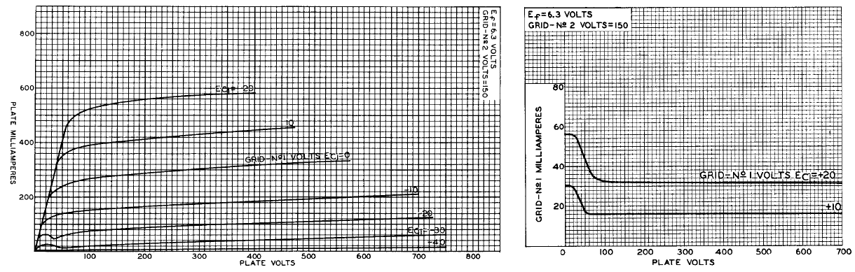
Figure 0.1 Few graphs from the 6146B datasheet.
After having recovered from the uTracer4 debacle (not really, I learned a lot from it) it became time to start thinking of a new design that would fulfil some of the wishes of demanding users. Readers who have followed my “uTracer Lab Notebook” will have noticed that I have been tinkering with ideas for an extended grid bias supply that can do negative as well as positive voltages, and a programmable buck converter heater supply. The remaining problem is how to realize an high voltage supply capable of higher voltages and currents with cheap easy to get components that is still so robust that it can withstand complete short circuit conditions. But what voltages and currents?
A few weeks ago somebody gave me a couple of 6146B beam power tubes. Searching the internet I discovered that the 6146B is a very popular transmitting tube used by radio amateurs. On studying the 6146B data sheet I found that this is the kind of tube that would really need all the new features I have in mind for a possible uTracer5! Voltages up to 800 V, currents in excess of 500 mA, and both positive and negative grid biases. So I decided to take the set of curves of Fig. 0.1 as a kind of target for the uTracer5 specifications. Obviously, I already have been doing some thinking and back of the envelope calculations to estimate what is reasonably possible and from this I come to the following tentative uTracer5 specifications:
The disappointment over the uTracer4 project, in combination with the experience gained in the uTracer3+ development set me thinking to find a way to extend the uTracer3 concept to much higher voltages. The work on the high voltage switch for the uTracer3+ had convinced me that as long as the response time of the switch is fast enough, a short circuit proof high-voltage supply is feasible, even for much higher voltages. The biggest challenge in extending the uTracer3 concept to higher voltages lies in finding suitable electrolytic capacitors and pnp transistors with working voltages in excess of 450 V. At the same time it should be mentioned that working voltages of 450 V to 500 V already stretch the capacity of a simple boost converter as used in the uTracer3 to the limits.
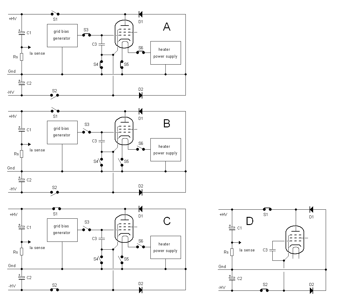
Figure 1.1 First (quickly rejected) idea to use voltage doubling to obtain higher voltages.
The path towards the conception of a new idea is never a straight line but often takes many turns and twitches into dark alleys before the true light is seen. An example of such an, in hindsight, not so good idea
is shown in Fig. 1.1. The idea was to use two boost converters, a positive and a negative one, to obtain the double working voltage of what can be achieved with a single boost converter, so in total 800-900 V. In the standby situation (Fig. 1A) the heater is active and a grid bias capacitor is charges to the required grid bias voltage. Next S3 ... S6 are opened (Fig. 1B). The tube now becomes floating with respect to ground, but the control grid voltage is “remembered” by C3. During the actual (pulsed) measurement S1 and S2 are closed applying a positive bias to the anode and a negative bias (with respect to ground) to the cathode, the grid still being biased by C3 (Fig. 1C and 1D). Note that diodes D1 and D2 prevent reverse biasing of the high voltage switches beyond their working voltages.
Capacitor stacking
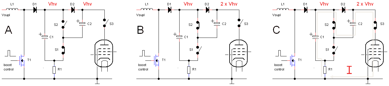
Figure 1.2 Basic idea of voltage doubling by stacking of capacitors
An invaluable sparring partner as far as power conversion issues are concerned is my colleague Peter Blanken. In discussing with him the idea sketched above we quickly came up with a number of issues and problems. It was Peter’s idea to implement the idea of using two boost converters in a completely different way, namely to use only one boost converter to charge two capacitors and subsequently stack the capacitors! The idea is illustrated in Fig. 1.2. In the charge phase S1 is closed and S2 and S3 are open (Fig. 1.2A). In this situation the boost converter consisting of T1, L1 and D1 charges C1 and through D2 capacitor C2 to a voltage Vhv. A fraction of a second before the actual measurement pulse S1 is opened and S2 is closed (Fig. 1.2B). Diode D2 now becomes reverse biased and since both capacitors are now in series, the voltage on the cathode side of D2 increases to 2*Vhv. During the actual measurement pulse S3 closes (Fig. 1.2C). The colored line in Fig. 1.2C gives the path of the current during the measurement. As can be seen, all current passes through R1 so that again the voltage drop over R1 is a perfect measure of the current through the tube.
Note that by stacking the two capacitors the resulting capacitance is half of that of a single capacitor. Since the total effective capacitance of the reservoir capacitor determines the voltage drop during a measurement pulse this implies that the voltage drop is doubled. A good question is how serious this is? In the uTracer3 the capacitance of the reservoir capacitor is 100 uF. With a maximum current of 200 mA and a measurement pulse length of 1 ms this results in a maximum voltage drop of V = (I*t)/C = (0.2 mA * 1 ms) / 100 uF = 2V. So halving the capacitance will double the voltage drop. Is this serious bearing in mind that the capacitor voltage is measured after the measurement? Then again perhaps it is very well possible to reduce the length of the measurement pulse. In short a topic for further consideration!
Double half-H bridges
The very elegant scheme of Fig. 1.2 makes it possible to achieve double the voltage of the standard boost converter using only “standard” 450 V capacitors, but it doesn’t eliminate the need for a 900 V, or with a safety margin, 1000 V switching device. As discussed above, it is very difficult to find affordable PNP or PMOS devices for these working voltages. However, NPN and NMOS devices for these voltages are readily available. In general N-type devices require a more complex driver circuit because the gate voltage has to be controlled with respect to the source which is floating and even has to become higher than the high voltage rail when the device is fully on! As it turns out, for this application, also the P-type solution would require a special driver scheme to galvanically isolate the high voltage switch from the rest of the circuit, so in complexity there is not much difference. Finally we have to make the choice between an NPN bipolar transistor or an N-Channel MOSFET. Given the fact that for the MOSFET we don’t have to bother with a static gate current and that suitable high-voltage NMOS transistors are relatively cheap the choice was easy. At first sight suitable transistors are the FQD2N100 from Fairchild or the STD2NK100Z from ST Microelectronics. These transistors have an on resistance of resp. 9 and 6 ohm, more or less independent of the drain current, so that it is quite straightforward to compensate for the voltage drop over the transistor after the measurement.
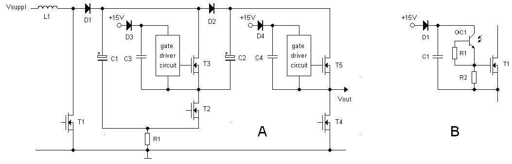
Figure 1.3 Schematic implementation of the capacitor stacking idea using two half-H bridges.
The idea is to power the driver circuit with a classical bootstrap circuit. Figure 1.3A shows a more detailed version of the circuit of Fig. 1.2A where the ideal switches have been replaced by NMOS transistors. With respect to Fig. 1.2 an additional switch in the form of T4 has been added. In the charge- or standby situation T2 and T4 are both on. In this mode not only C1 and C2 can be charged, but also the sources of T2 and T5 are pulled to ground potential. In this situation diodes D3 and D4 conduct and charge bootstrap capacitors C3 and C4 to 15 V. Immediately prior to the actual measurement T2 and T4 are switched off, and T3 is switched on followed by T5. After a few milliseconds T3 and T5 are switched off again. Capacitors C3 and C4 are dimensioned in such a way that they hold enough charge to power the driver circuit during the whole cycle. The whole circuit consists in fact of two so called half-H bridges, used in a somewhat unusual circuit configuration, hence the name “double H-bridge circuit.”
The gate driver circuit itself could be simple as the circuit shown in Fig. 1.3B. Similar to the uTracer3 high voltage an opto-coupler is used to drive the high voltage transistor while at the same time the driver circuit is galvanically isolated from the rest of the circuit, a prerequisite for an accurate current measurement.
The ground reference
Boost converters have the (sometimes) undesirable property that the minimum output voltage is limited to the supply voltage. To allow the boost converter to charge the reservoir capacitors to the maximum voltage in a reasonable time, the boost converters are operated at a relatively high voltage of 19.5 V which conveniently coincides with the voltage of laptop supplies. This implies that the minimum high voltage would be limited to 19.5 V! In the uTracer3 therefore, the cathode of the tube is not referenced to the power supply voltage rather than to ground. For a number of reasons however I would like to have the cathode referenced to ground.
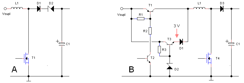
Figure 1.4 Two way to make a boost converter “under perform.”
I know of two tricks to modify a boost converter so that output voltage can be lower than the supply voltage. The simplest method is shown in Fig. 1.4A. By simple inserting a zener diode with a breakdown voltage higher than the supply voltage in series with the boost converter diode, the supply voltage is effectively blocked, and the output voltage can now be adjusted down to 0 V! This very simple method has the disadvantage that a certain amount of energy is dissipated in the zener diode. This inevitably will result in a longer charging time of the capacitor and thus a longer measurement time.
In the second method a second power supply s used with a very low voltage for example 2 V. Figure 2Bshows a circuit implementation of this idea. The very simple voltage regulator consisting of T3, R3 and D2 generates a voltage of approximately 3 V. For output voltages higher that the supply voltage T1 is switched on so that the boost converter is supplied directly by the 19.5 V power supply. For output voltages lower than the supply voltage T1 is switched off. The boost converter input voltage now drops to approx. 2 V. In this way it is possible to obtain output voltages as low as 2 V at the expense of some additional circuitry and two (also one for the screen supply) control lines.
Discharging
We should almost forget that also a means to discharge the capacitors needs to be implemented to discharge the capacitors when e.g. a new curve is measured of when the measurement is finished. The simplest way to implement this is to use a simple discharge resistor and tranistorin the same way as this is done in the uTracer3 (Fig. 1.5A)
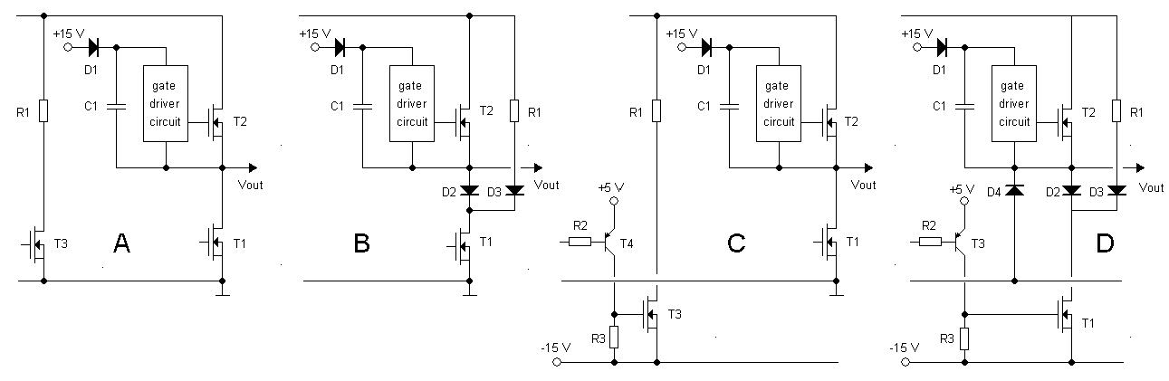
Figure 1.5 Different implementations of the discharge circuit.
However, it seems rather a waste to use an additional transistor for that while we have another high voltage switch in almost the same “position” doing nothing most of the time: transistor T1 only needs to be closed a few milliseconds just before a measurement pulse! With a simple “OR” circuit consisting of diodes D2 and D3 we can let T1 perform the two tasks of discharging the reservoir capacitors and grounding of high side driver circuit so that the boots-trap capacitor can be charged. In a different way the discharge transistors in the uTracer3 also perform the dual functions of discharging and charging the driver circuit.
With the reference potential at ground level, it will become difficult to discharge the capacitors to 0 V because of course with a resistor the discharging decays exponentially. A better idea is to discharge the reservoir capacitors to a negative potential (Fig. 1.5C). With three diodes it is again possible to combine T1 and T3. The logical “OR” diodes D2 and D3 pull de boost converter and the discharge resistor down, while D1 prevents that the source of T2 can become negative.
To keep in mind When during discharging the voltage on the capacitors drops below half the maximum voltage, the discharging can be accelerated by stacking the capacitors. This will double the voltage and half the capacitance! However, continuous stacking of the capacitors is not possible because the boots-trap capacitors only hold a finite amount of charge. Still some kind of pulsed scheme might be created whereby the capacitors are mostly stacked shortly interrupted my very short moments in which the boots-capacitors are charged. Sounds complicated, bt a piece of cake for a micro-controller!
A first version of the complete circuit
In the figures below a first plan for a single pulsed high-voltage supply with stacking is sketched. So far all mainly based on ideas and so far a few, but very little experiments.
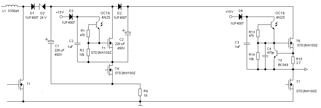
Figure 1.6A The basic double half H-bridge
Figure 1.6A shows the backbone of the capacitor stacking circuit. A zener diode is used the allow for output voltages down to 0 V. Experiments show that, especially in a multi-point curve, the increased charging time as a result of dissipation losses in the zener diode can be neglected. The control circuit of the left half H-brdige is straight forward. The control circuit of the right half H-bridge contains a classic current limiting circuit consisting of T5 and R15. The control circuits will be tested in the next section.
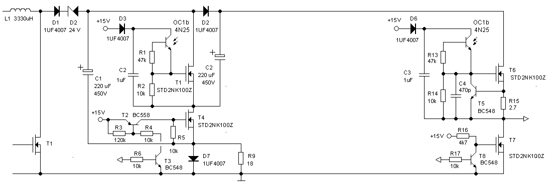
Figure 1.6B Gate driver circuits of the low-side transistors added.
The high-voltage MOSFETs have a somewhat higher threshold voltage, and to ensure that they are fully on, the gates are controlled by a separate driver transistor. This has the additional advantage that, if needed, the turn-on time of the MOSFETs can be increased by increasing R5 and/or R16. A possible danger is that the potential on the drains of the low-side transistors drops so fast that as a result of the inevitable gate-drain capacitance of the high-side transistors, the gate-source voltage increases for a short moment the threshold voltage so that both transistors are on at the same time!
The driver circuit of T4 has also a second, even more important, reason: during the actual measurement, the current through the current sense resistor R9 will cause a negative voltage drop over this resistor, also making the source of T4 more negative. Remember, that during a measurement this transistor if off. The negative voltage on the source could very well cause the transistor to turn on! In the proposed circuit R5 keeps the gate-source voltage zero as long as T2 is not on,even if the source of T4 is pulled negative. Diode D7 ensures that the source of T4 can never become more positive than 0.8 V during charging of the reservoir capacitors.
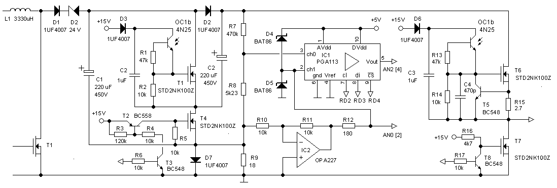
Figure 1.6C Voltage and current Measurement circuit added
This part of the circuit is nearly identical to the circuit used in the uTracer3. Low-offset OpAmp IC2 inverts the negative voltage drop over R9 which is a measure for the current. This results in a voltage between zero and 5 V for the highest current measured. The output of IC2 is directly applied to one of the analog inputs of the PIC where it is used to sense an over-current situation during a measurement pulse by means of a very fast processor interrupt. The signal is also fed into one of the inputs of a Programmable Gains Amplifier (IC1) for scaling of the measured current before the signal goes into the AD converter on-board of the PIC.
The high-voltage needs to be measured at two moments:
1. During charging of the reservoir capacitors.
2. Directly after the measurement, to measure the best possible estimate of the applied voltage during the measurement pulse itself.
Both measurements can be performed best by measuring the voltage of C2, after diode D2. Note that during charging the voltage range on this point is 0 – 450 V, while directly after the measurement the voltage range will be 0 – 900 V. The voltage divider therefore needs to be dimensioned for the high value. The measurement accuracy of the low voltage range therefor drops. To compensate for this the second channel of the PGA is used! Note that the “bottom side” of the voltage divider is reference to R9 rather than to ground. The reason is that referencing to ground would add the current to the measurement current. Drawback is that the high voltage cannot be measured during a measurement pulse because the current though R9 would offset the measurement.
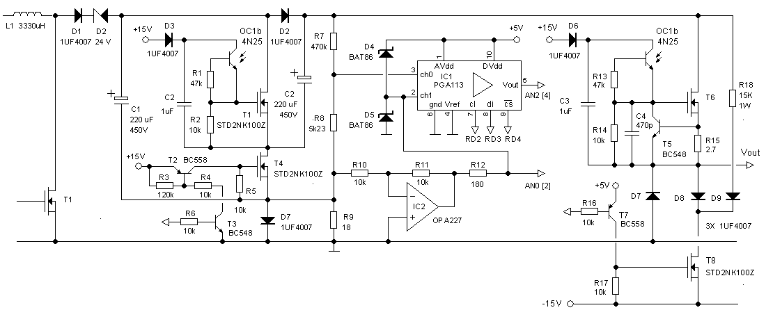
Figure 1.6D Discharge circuit added
The discharge circuit is, as discussed, referenced against a negative voltage to ensure fast and complete discharging even for low voltages. It may even be possible to reference the circuit against the raw negative voltage (-30 V ?). However, that will require some additional provisions to ensure that the maximum gate-source voltage does not exceed 20 V.
| to top of page | back to the uTracer homepage |
The most critical part in the new high voltage supply circuit discussed in the previous section is without doubt the high voltage switch circuit around T6, T5, OC1b in Fig. 1.6D. It is this circuit that has to switch on and off the high voltage, limit the current in case of an overload or even short circuit, and switch off the load in case of an overload condition fast enough to prevent damage to the circuit. In this section the high voltage switch will be analyzed and tested to find out its operating limits.
Figure 2.1 Test circuit for the NMOS high voltage switch
Analzing and testing an “high-side” circuit like the high voltage switch is usually not that easy. All the components are at a high potential with respect to ground and complicated differential probes have to be used to measure e.g. a gate-source voltage. Fortunately, since the control input of the switch is basically isolated from the rest of the circuit through the use of an opto-coupler (the bias diode D2 Fig. 2.1 is normally off), it is possible to exchange the position of the load and the switch with respect to ground so that the circuit can be tested using ground as a reference.
Figure 2.1 shows the test circuit used in this section. Going from left to right we first Find a pulse generator which simulates the measurement pulse normally issues by the PIC. It consists of a de-bounce circuit around N1 and N2, the pulse generator consisting of C1, R3, D1 and N3, and a buffer that eventually drives the LED in the opto coupler consisting of N4-N7 and T1. The pulse length is determined by C1 and R3. A 1 nF capacitor generates a 10 us wide pulse which is approximately the pulse width when the processor interrupts the measurement because an over-load condition has been detected. A 150 nF capacitor results in a pulse length of approximately 1 ms, the normal measurement pulse length. The reservoir capacitor consists of two 220 uF / 450 V capacitors in series. Resistors R6 and R7 ensure that the high voltage is distributed evenly over both capacitors. The current is measured over Rsense. That that this causes a negative voltage drop over the resistor. The reservoir capacitor is charged via R9 by my (very) high voltage supply consisting of three stacked delta E0300-0.1-L 0 – 300 V power supplies, capable of generating 0 – 850 V. The voltage over the high voltage switch is measured with a 10:1 voltage divider (and a 10:1 scope probe). The zener diode is used for Ron measurements to prevent overloading of the scope input.
The operation in detail
The high voltage switch can operate in three different modes:
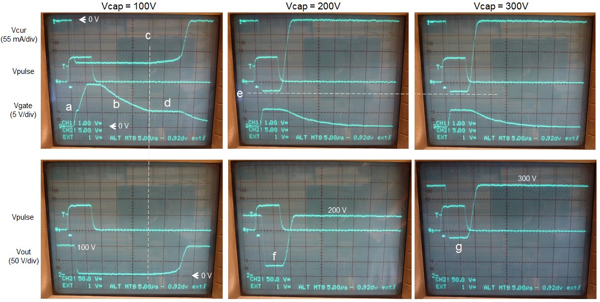
Figure 2.2 Analysis of the waveforms in the NMOS high voltage switch (see description below).
In Figure 2.2 the working of the switch in modes 2 and 3 is analyzed. For safety reasons the voltage is not pushed to the limit, but a maximum voltage of 300 V is used. The figure shows in three columns three different voltage setting: 100 V, 200 V and 300 V. The pictures in one column show different signals during the same measurement. The center trace in both pictures is the pulse signal that is also used to trigger the scope. In this case the pulse width is ca. 8 us. The upper trace in the top pictures shows the Vcur which is the voltage drop over Rsense. The lower trace in the top pictures shows the gate voltage of the NMOS. The bottom trace in the lower picture shows the output voltage. Because the switch circuit has been shifted to ground level, the output voltage is high in the off-phase and should approach zero in the on-phase.
As load a resistor of 800 ohm is used. This means that with increasing voltage and the hardware current limit set at 250 mA (Rcur = 2.7 ohm), the hardware current limit protection will kick in at around V = R*I = 800*0.25 = 200 V. For 100 V the hardware current limit circuit is not yet activated. After the start of the measurement pulse, the photo transistor in the opto-coupler is switched on, and the gate voltage rises. The rise time is limited by the current the photo transistor can generate and the gate capacitance of the MOSFET. At Around 5 to 6 V gate voltage, the MOSFET switches on (Fig. 2.2a) and the output voltage drops. The sharp decrease of the anode voltage counter acts (through the drain-gate capacitance) the charging of the gate resulting in the kink in the gate voltage. Eventually the gate voltage rises to 15 V and the MOSFET is fully on. After the measurement pulse has been switched off, the gate is discharged by resistor R9 resulting in a logarithmic decay of the gate voltage (Fig. 2.2b). Since during that time the gate voltage is higher than the threshold voltage, the MOSFET remains fully on. At point c the gate voltage approached the threshold voltage and the MOSFET starts being switched off causing an increase in anode voltage. The increasing drain voltage, again through the drain-gate capacitance, counter acts the discharging of the gate and actually stabilizes the gate voltage on a plateau value around the threshold voltage (Fig. 2.2d). At a certain point this balance situation can no longer be maintained and the MOSFET is finally switched off.
At 200 V the hardware current limit circuit has kicked in (Fig. 2.2 middle column). Note that the drain voltage in rest is 200 V, and but that during the measurement pulse the drain voltage is no longer zero but has increased to approximately 80 V (Fig. 2.2f). This is because the hardware current limit circuit has regulated the conduction of the MOSFET in such a way that it is now dropping these 80 V so that the current through the load remains constant at 250 mA. As a result the gate voltage is adjusted to a value slightly above the threshold. Since the gate voltages is already around the threshold voltage, and the drain voltage is no longer zero, the switch-off time is drastically reduced. For 300 V the current remains constant (Fig. 2.2e), which is only possible by allowing for a higher voltage drop over the MOSFET (Fig. 2.2g).
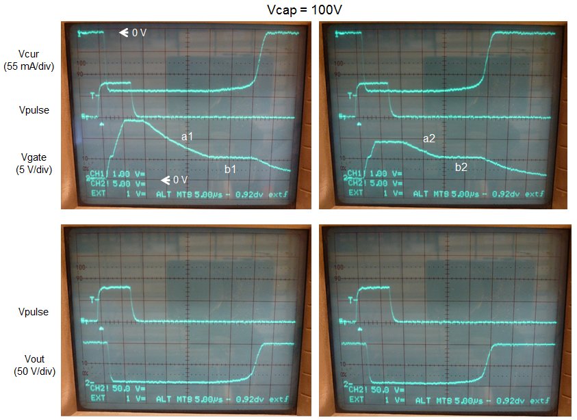
Figure 2.3 Switching characteristics at Vgate = 15 V (left column) and Vgate = 10 V (right column).
Figure 2.3 shows a similar set of curves as in Fig. 2.2 for a voltage of 100 V and a load resistor of 800 ohm (current limit circuit not activated). In the left column a gate voltage of 15 V is compared to a gate voltage of 10 V in the right column. By decreasing the gate voltages the discharging of the gate is significantly reduces (comp. a1 to a2 in Fig. 2.3) However, the plateau time remains the same (comp. b1 and b2). A gate voltage of 10 V seems optimal.
Pulse testing @ 550 mA
During the first tests it appeared that the NMOS high voltage switch easily passed all load and short circuit tests with the hardware current limit set to 250 mA. The hardware current limit was therefore set to 550 mA by lowering Rcur to 1.189 ohm (2.7//2.7//10).
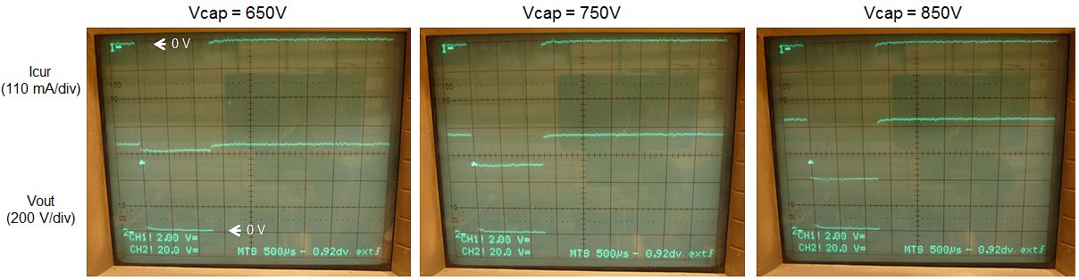
Figure 2.4 Mode 1 testing at 550 mA (load = 1k5).
The first test was for normal operation with a measurement pulse length of 1 ms. Figure 2.4 shows the current as well as the drain voltage of the switch connected to a load resistor of 1k5. The load resistor was chosen such that the current limit circuit would just come into action between 750 and 850 V. The graphs show a perfect switching behavior even for the highest voltage and current combination.
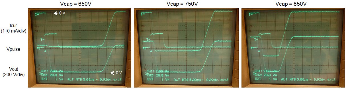
Figure 2.5 Mode 2 & 3 testing around 550 mA (load 1k5)
In the second test Mode 2 and 3 operation is simulated with a mesurment pulse length of 10 us. A load of 1k5 is connected and the voltage is increased from 650 to 850 V (Fig. 2.5). At 650 V the hardware current limit circuit is not yet activated, the gate voltage of the MOSFET of 15 V, and the turn-off time is relatively long. At 750 V the current limit circuit is just activated and the pulse length is decreasing. At 850 V the current limit circuit is fully activated, the gate voltage is around the threshold and the turn-off time is minimal. The current is 550 mA.
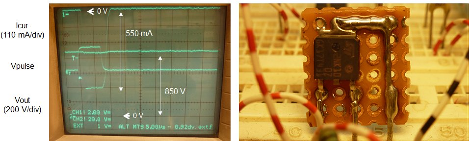
Figure 2.6 Full short circuit test at maximum voltage (850 V) and 550 mA! The tiny MOSFET in DPAK package is capable of handling an instantaneous dissipation of 425 W!
Finally a full short circuit test at maximum voltage (850 V)and maximum current (550 mA). Figure 2.6 shows how the tiny MOSFET handles an instantaneous dissipation of 425 W repeatedly without problems.
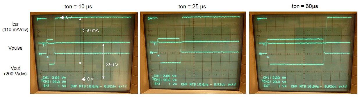
Figure 2.7 Exploring the safety margin
To investigate the safety margin we have with this switch circuit, the pulse length was increased in steps at maximum voltage (850 V) and full short circuit conditions (Fig. 2.7). It appeared that the pulse length could be increased to at least 60 us – 6 times the pulse length in reality – without problems. Most likely I could have gone further, but since this is evidence enough to convince me of the robustness of the circuit, and since I don’t like pushing buttons and waiting for a bang, I didn’t push it any further.
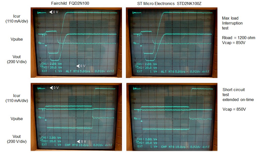
Figure 2.8 The FQD2N100 compared to the STD2NK100Z.
There are two 1000V MOSFETs that are readily available and reasonably priced: The FQD2N100 from Fairchild, and the STD2NK100Z from ST Micro Electronics. Their datasheets are pretty similar. The main difference is their price: the STD2NK100Z is about doubke the price of the FQD2N100. Under the assumption that more expensive also implies better performance all experiments so far were carried out using the STD2NK100Z. However, the comparison of the two in Fig. 2.8 shows that both transistors show almost identical behavior and that FQD2N100 even shows slightly better turn-off characteristics.
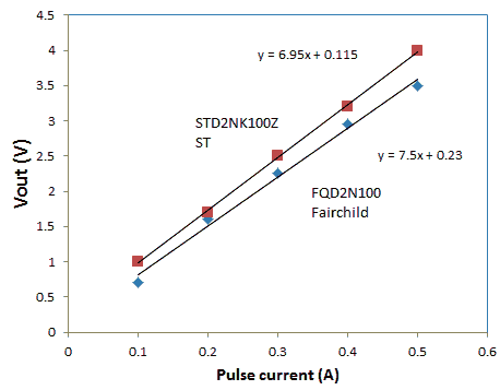
Figure 2.9 Voltage drop over the MOSFETs as a function of drain current.
The voltage drop over a bipolar transistor in saturation is usually more-or-less independent of the current, and usually amounts to 100 to 200 mV. A MOSFET in the on-state in contrast behaves as a resistor with the on-resistance a function of the gate voltage. The voltage drop over the MOSFET will therefor depend on the current. This is not a problem, since – just as with the uTracer3 – the plotted current can be corrected for this voltage drop. To measure the on-resistance of the MOSFET, the voltage drop over the MOSFET (+ 2.7 ohm resistor) was measured for different currents taking care that the current limit circuit was not activated. To measure the Ron, the output voltage of the output voltage divider was limited to 2.7 V by means of zener diode D3 (Fig. 2.1). This allows for zooming into the low voltage drop when the MOSFET is on, while the input voltage is clipped when the MOSFET is off so that the amplifier of the oscilloscope is not saturated. The Ron (corrected for the 2.7 ohm resistor) has been plotted versus the current for both type MOSFETs in Fig. 2.9. The on-resistances for both types are indeed more or less constant and correspond well to the values specified in the datasheets.
| to top of page | back to the uTracer homepage |
Tackling dV/dt breakdown
While playing with the HV-switch test circuit (Fig. 2.1) a rather startling incident/accident occurred. I had the load resistor connected with two (isolated) clips, and at a certain moment I disconnected the load while the reservoir capacitor was charged to 900 V and T3 was not conducting. The moment I opened the clip, there was a big bang the MOSFET, Rcur, Rsense, and a fuse I had in series with the capacitor were blown to pieces (Fig. 3.2)! What on earth had happened, and how can opening of a circuit result in such a violent event?
The most likely explanation is a dV/dt breakdown. Such a breakdown can occur when the rate of increase of the drain voltage exceeds a certain value. What happens is that the drain-gate capacitance causes a positive transient on the gate which not only momentarily opens the MOSFET, but which also may very well destroy the gate oxide causing the MOSFET to permanently fail. When I opened the clip I must have accidentally touched the lead resulting in a dV/dt breakdown. So, what measures can be taken to prevent the occurrence of such an event during use of the circuit in the tube tester?
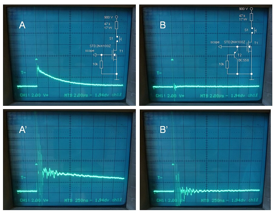
Figure 3.1 dV/dt testing without gate driver circuit (AA’) and with push-pull gate driver (BB’).
A simple experiment was used to get an qualitative idea of the impact of a buffer circuit on the dV/dt fenomenon. In Fig. 3.1A the drain of the MOSFET is connected via a push button and a current limiting resistor to a 900 V power supply. The signal on the gate of the MOSFET is monitored with a memory scope. When the switch is closed a transient appears om the gate. Figure 3.1A’ shows the same event on a different time scale. An extra transistor acting as an emitter follower almost completely suppresses the transient (Fig. 3.1B and B’). At t=0 there is in all cases a very large and very short spike that doesn’t decrease in amplitude when a buffer is used. I think is has nothing to do with the dV/dt effect but is just a measurement artifact.
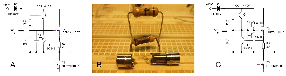
Figure 3.2 A) Original HV-switch circuit, B) collateral damage as a result of a dV/dt breakdown, C) new HV-switch circuit with gate driver.
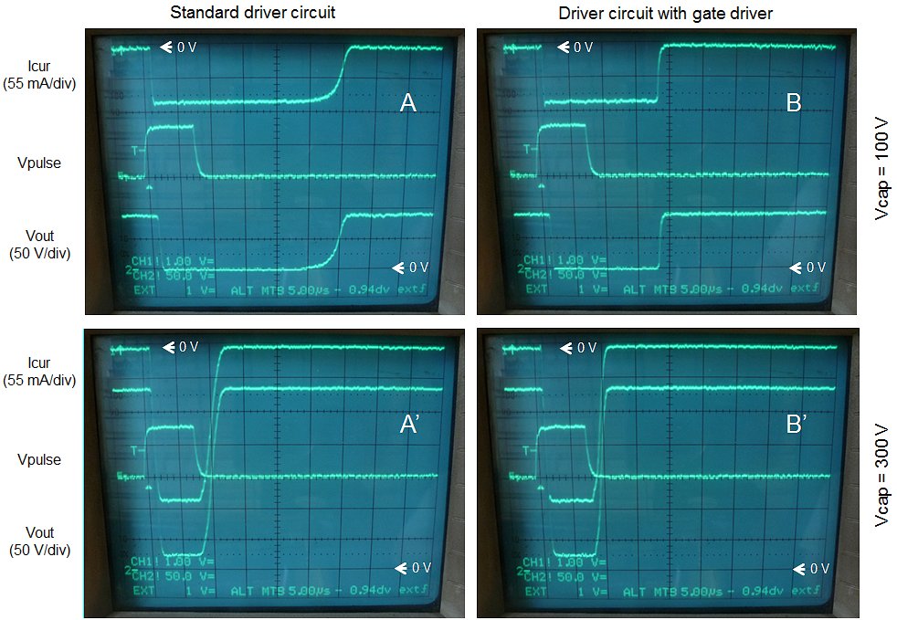
Figure 3.3 Switching behavior of the new HV-switch circuit compared to the standard circuit. Rload = 1 kohm
In the HV-switch circuit shown in Fig. 3.2C, a push-pull buffer circuit has been added to provide a low impedance drive circuit for the gate of the MOSFET. This does add some complexity to the circuit, but it greatly suppressed dV/dt related problems, while it also improves the switching speed of the circuit especially the turn-off time. This is illustrated in Figure 3.3. Here the switching behavior of the standard circuit (left two photos) is compared to the circuit with the buffer stage (right two photos). In the top two photos the hardware current limit is not activated, while it is activated in the bottom two measurements. Especially in the case when the current limit is not active the reduction of the switch-off time is significant because the discharge of the gate-source capacitor is faster (Figure 2.3 part a1). However, the typical MOSFET turn-off behavior/time when the gate voltage passes through the Vt (Fig. 2.3 part b1) still remains.
Pulse testing @ 1 A!
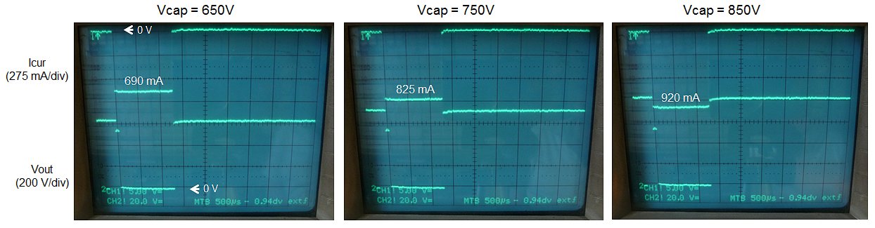
Figure 3.4 Standard 1 ms test. Rload = 900 ohm (1k//10k), Rsense = 2.7/4 = 0.65 ohm
During experiments with the HV-switch with the push-pull gate driver it was observed that the new circuit was much more stable in the current limiting regime. The 470 pF capacitor could be omitted without any problems and only for very low voltages oscillations were observed which readily disappeared for voltages higher than 100 V. It was therefore decided to again test the circuits up to currents of 1 Ampere! To set the hardware current limit to 1 A , Rsense was replaced by four 2.7 ohm resistors in parallel. Figure 3.4 shows the one millisecond Mode 1 test for voltages and currents around the maximum values. With a load resistor of 900 ohm and a voltage of 850 V, the circuit is tested at maximum voltage and maximum current. At the highest current the discharging of the reservoir capacitor is clearly visible
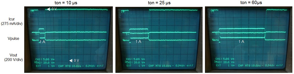
Figure 3.6 Full short circuit test extended times. Rsense = 2.7/4 = 0.65 ohm
Figure 3.5 Shows the high-speed switching behavior around the current limit region. The switching of 1 Amp at 900 V is no problem at all for the circuit. The switching speed is very fast, and the total on-time is very much determined by the control pulse width.
Finally, the robustness of the circuit was tested under full short circuit conditions at maximum voltage for extended times. The circuit easily managed to cope with repeated blasts at 60 us without problems!
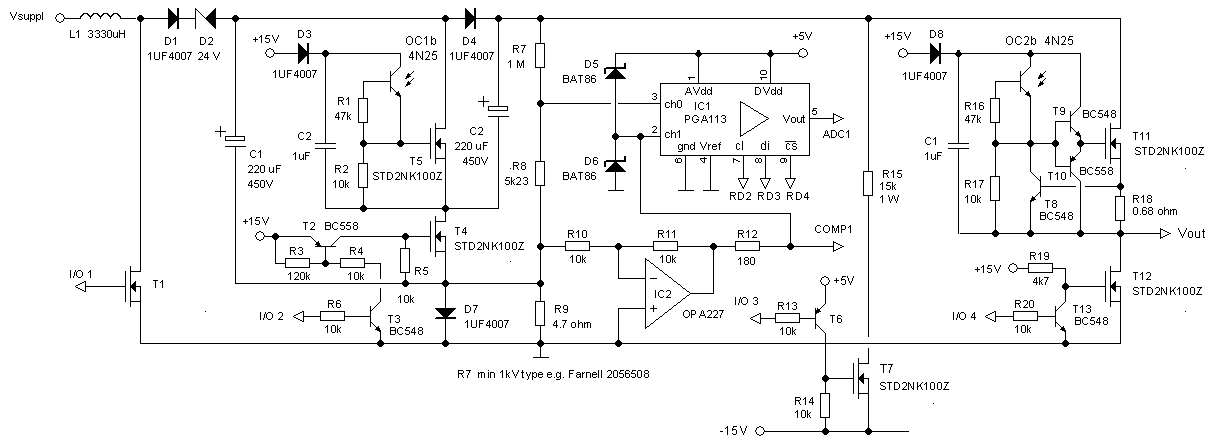
Figure 3.7 Improved high voltage 900 V / 1 Ampere supply circuit.
Figure 3.7 shows the circuit diagram of the 900 V / 1 Ampere high-voltage switch in which the latest insights have been implemented. In this version a separate transistor is used to discharge the reservoir capacitors so that the T12 can be on in between measurements so that the output is always at ground potential and not floating. The high voltage switch MOSFET has a push-pull gate driver circuit, and the current sense resistor has been decreased to 4.7 ohm to accommodate the higher current. At first sight the circuit looks rather complex, but in reality it is (apart from the OPA227 and PGA) just a hand full of very ordinary off the shelf discrete components delivering extraordinary performance!
| to top of page | back to the uTracer homepage |
After these very promising first tests, it is time to test the complete circuit under realistic circumstances. A great advantage of this circuit is that it, in contrast to the version 4 HV circuit, greatly resembles the uTracer 3 high-voltage supply. To combine the new circuit with the existing hard- and firmware really only a few additional control signals are needed.
A test bench was built using as much as possible of the uTracer3 hard-and software combined with a single new high-voltage supply. A standard uTracer3 PCB was equipped with the processor, positive and negative power supplies and a single PGA113/OPA277 section. The screen supply section was not used, and the I/O’s which became available from that section were used as the additional control signals needed for the new HV supply.
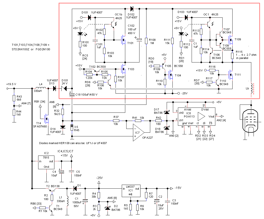
Figure 4.1 The circuit diagram of the HV voltage source test-board. The part of the circuit within the red frame can be found on the perf-board, the rest of the circuit is on an uTracer3 PCB.
Figure 4.1 Shows the schematic of the test circuit. The part of the circuit in the red box is new, while the part of the circuit outside the red box has been taken directly from the uTracer3 with only a few modifications. In the first place the negative power supply has been lowered to -25V by lowering R4 to 30k. It is the idea to use a double grid supply in a new uTracer design with one grid supply for the +100 V to 100 V range, and a second simple supply for the 0 to -20 V range. The last range is generated by a single OpAmp and a negative supply voltage of -25 V is perfect for that. Additionally the -25 V is used to discharge the reservoir capacitors down to 0 V by means of T104. Here the combination of the +5 V and the -25 V supply just provide the voltages to control the gate of the MOSFET within the maximum gate voltage range. Note that this lower negative supply voltage makes it additionally possible to use a simple LM7915 for the -15 V supply. A second modification the uTracer3 board is that the tube is no longer referenced to the positive supply voltage but to ground!
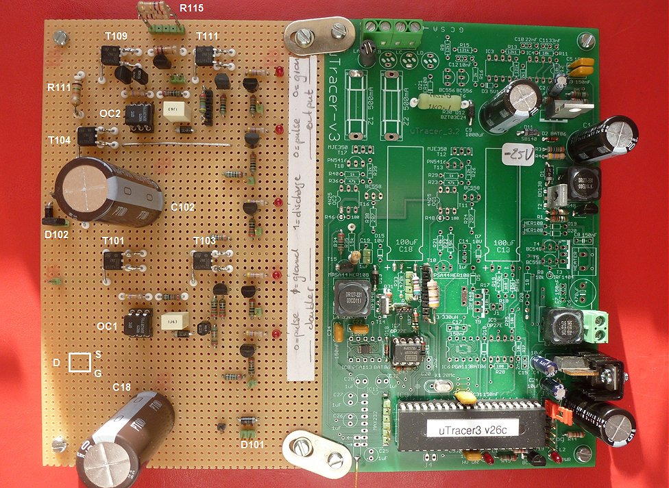
Figure 4.2 The test board bathing in the Sunday morning sunshine. Click Here for a photo of the backside of the board.
The part of the circuit within the red box pretty much contains the final circuit as presented in the last section (Fig. 3.7). There are only a few small modifications. The most important one is related to the gate control of T103. In the circuit of Fig. 3.7 a resistor between gate and source was used to close this transistor when it is not on. However, for high currents the voltage drop over the sense resistor can be almost 5 V, making the source of T103 also 5 V negative. This tended to open the transistor for high currents. Tying the gate pull-down resistor to -25 V solved the problem. The second modification is that the discharge transistor has been directly tied to -25 V instead of -15 V. This provides faster discharging while it prevents unnecessary loading of the -15 V regulator resulting in a cleaner negative supply voltage.
The firmware
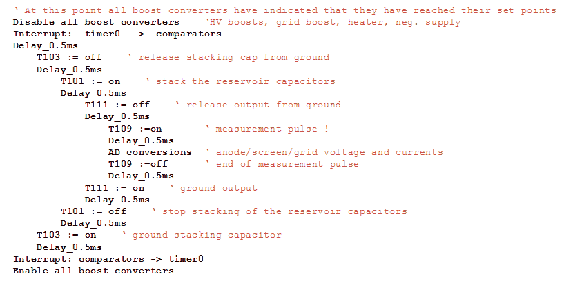
Figure 4.3 Control of the HV switch.
Although for “a real” version 5 the firmware will be thoroughly revised, it was fortunately possible to get the new HV-supply working with minimal modifications to the uTracer3 firmware. Most important was the addition of a number of I/O’s to control the MOSFET switches. The pseudo code in Fig. 4.3 shows how these control signals are generated. A measurement event starts with the stacking of the reservoir capacitors. This itself consists of two steps: release of ground to the stacking- and bootstrap
capacitors, and the generation of the measurement pulse itself which also consists of two steps: release of ground to the bootstrap capacitor and output, and the switching-on of the final output switch. Between all steps at this stage a delay of 0.5 ms has been inserted to be sure that the circuit stabilizes after every step, and to allow for easy tracing of the signals on the scope. In the final version 5 all of these control signals may be shared between anode and screen supplies. However, since the screen voltages are usually much lower than the anode voltages it may be advantageous to have the stacking control signals separate.
Compliance setting
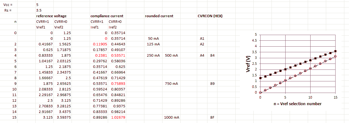
Figure 4.4 Selection of compliance values
The selection of the proper value for the current sense resistor (R45 in Fig. 4.1) is a compromise. Ideally we want to select the resistance is high as possible for a maximum sensitivity and signal to noise ratio. In other words a voltage drop of 5V at the maximum current of 1 A, so 5 ohm. However, the voltage drop over this resistor is also used for compliance protection circuit where a comparator inside the PIC compares it with a programmable reference voltage also generated inside the PIC. Unfortunately the maximum voltage the programmable reference voltage source can generate is 3.6 V. For the current sense resistor therefor a value of 3.5 ohm is used. This will make it possible to set the compliance to 1 A. and additionally it is an commonly available resistor value. The programmable voltage source is rather an odd device that can generate, depending on the setting of a bit and a 4 bit value, a number of voltages. Figure 4.4 shows these voltages together with the corresponding compliance currents. From this list a number of settings more or less corresponding to the range: 50, 125, 250, 500, 750 and 1000 mA were selected. The values are not exact; that is not possible with such a simple solution or necessary either.
Demonstration of the HV supply
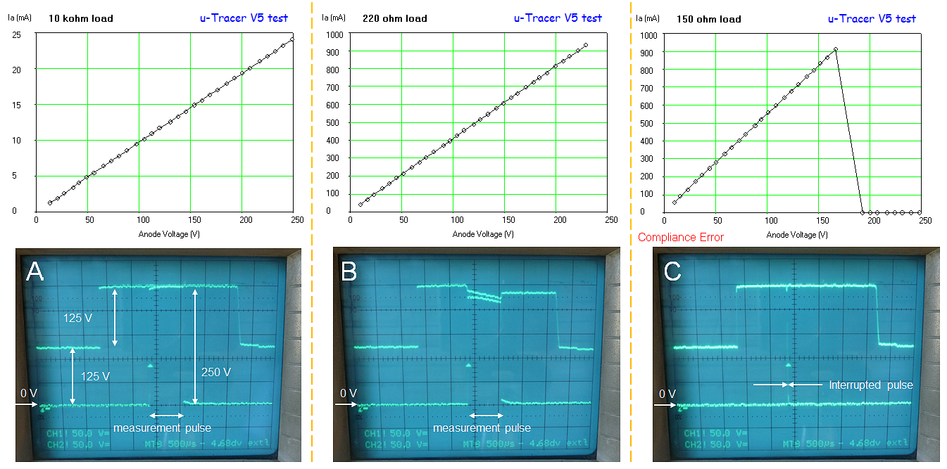
Figure 4.5 Working of the High voltage supply demonstrated
|
In Figure 4.5 the working of the high-voltage generator/switch circuit is illustrated. The upper trace in the figures shows the anode voltage of-C102 – the second reservoir cap -. The lower trace in the figures shows the output (pulse) voltage of the circuit that is normally applied to the anode (or screen). The columns in Fig. 4.5 represent a situation of: A: small load (low current), B: full load, and C: overload. In all the figures the measurement was a voltage sweep from 0 to 250 V with the scope image taken after the last measurement point (250V). Starting with Fig.4.5 A we see how the capacitors are charged to half the output voltage, 125 V. A few milliseconds before the measurement pulse the capacitors are stacked, lifting the anode voltage of C102 to 250 V. During the measurement pulse the 250 V is connected to the output of the circuit. Notice that the output voltage = voltage of C102. In Fig.4.5 B the circuit is loaded to almost 1 A. Looking at the upper trace we observe at the start of the measurement pulse a sudden (small) drop in voltage. This drop is caused by the voltage drop over the 3.5 ohm current sense resistor. During the measurement pulse the voltage of C102 decreases almost linearly as a result of the discharging of the reservoirs caps by the output current. At the end of the measurement pulse the voltage “jumps back” again a few volts because there is no voltage drop over the current sense resistor anymore. Looking as the output pulse in the same photo we see that the output voltage nicely follows the voltage of C102 be it that the output voltage is a few volts lower. This difference is caused by the approximately 5 ohm on-resistance of the MOSFET and the voltage drop over the overcurrent protection resistor. It is thus important that the voltage of the caps is measured as much as possible near the end of the measurement pulse, and that the voltage drop over the MOSFET and other resistances is taken into account. In the last column of Fig. 4.5, the compliance protection has been activated. The “output high” time is now so short that it is hardly visible on the trace. The working of the HV supply is also demonstrated in the video on the left. |
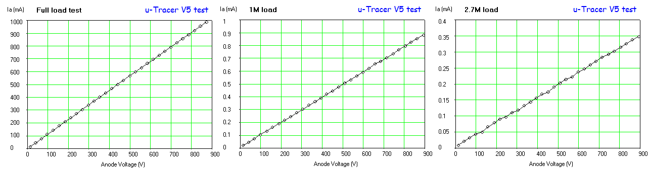
Figure 4.6 Four decades of current range
Figure 4.6 shows a series of measurements to get an impression how the circuit behaves on the lower end of the current range. In the uTracer 3 the current sense resistor was 18 ohm. In the current design the current sense resistor has been decreased to 3.5 ohm to allow for measurements up to 1 Amp. Inevitably this not only increases the current range at the high end, but it also decreases the sensitivity at the low end. Despite the fact that the construction of the test-board is not really ideal to reduce noise (Fig. 4.2), the left graph in fig. 4.6 shows that measurements in the range of 0-400 uA are still perfectly possible. By increasing the number of averages almost all measurements could be eliminated so that even measurements in the range 0-100 uA are possible.
Circuit update
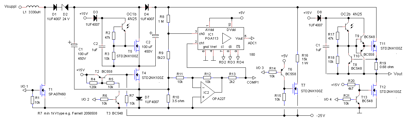
Figure 4.7 Updated high voltage supply circuit.
Figure 4.7 shows the updated version of fig. 3.7. With respect to fig. 3.7 the negative supply voltage has been decreased to -25 V, and the gate-sink resistor R7 has been connected to –25 V instead of to ground. The Schottky protection diodes D5 and D6 have been removed while resistor R13 (fig. 4.7) has been increased to 2k2 so that we can rely on the protection diodes at the input of the PGA113.
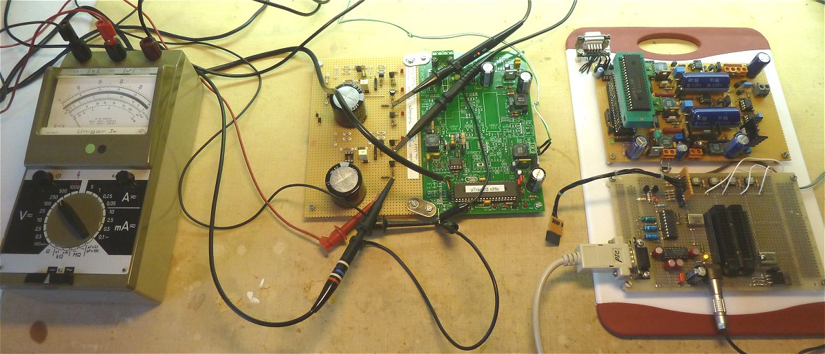
Figure 4.8 The test bench setup. From left to right: my reliable Unigor multimeter, the test bench itself with the new HV circuit on perfboard, and on the right my in-circuit PIC programmer + original uTracer3 circuit that I normally use to program and test PIC processors.
| to top of page | back to the uTracer homepage |
The previous sections discussed and demonstrated the principal ingredient of a 900 V uTracer, namely the high-voltage source and switch. In the meantime on my Lab Notebook page some other new building block for a “next generation” uTracer have been described such as a “bipolar grid supply” and a “DC Buck converter heater supply.” So now it has become time to piece the whole thing together, and come to a first circuit diagram of the uTracer 5. Unavoidably the circuit of the uTracer 5 will be more complex and larger than the uTracer 3. I will therefore partition the circuit into 5 parts: the CPU and DC power supplies (1), the heater and standard control grid supply (2), the bipolar grid supply (3), and the anode HV supply/switch (4) and screen HV supply/switch (5). Each circuit diagram has a number (the number between brackets) that is used to identify the components and the connections between the different circuit parts. So resistor R301 is resistor 1 in bipolar grid supply (3). I201>104 means a connection from point 1 on the heater circuit (2) to point 4 on the CPU diagram (1).
Heater and standard grid bias supplies.
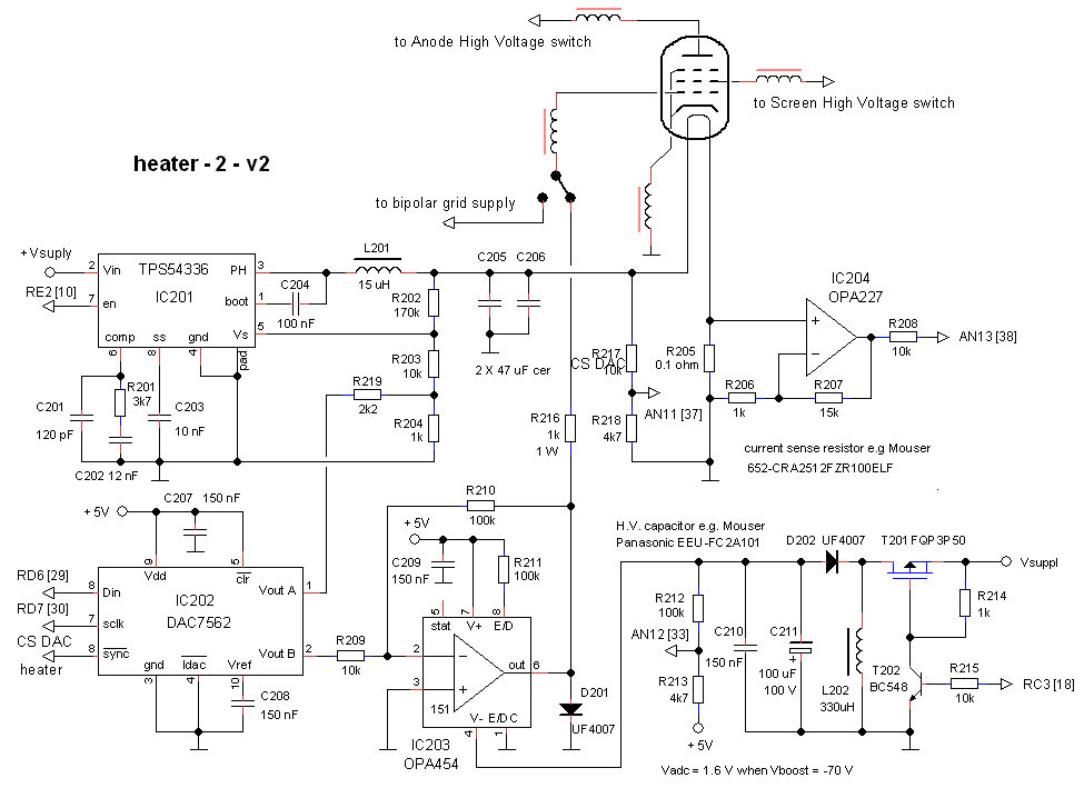
Figure 5.1 Heater and standard grid bias supplies.
A detailed description of the Buck converter heater supply can be found on the Lab Notebook Page. However, in the final design I selected a different DA converter namely the DAC7562 from TI. This IC has two separate 12 bit (!) DA converters including on-board reference, and uses a single SPI interface. One DA converter is used for the heater, the other for the negative grid supply. The output voltage of the DA converter can be programmed to values between true zero and Vdd (5 V). With the component values given in the circuit diagram the heater voltage can be set to any voltage ranging from 1.1 to 13.5 V.
The uTracer 5 heater circuit has been provided with a real measurement of the actual heater voltage and a current measurement arrangement. The voltage sensor simply consists of a resistive divider which directly feeds into one of the ADC inputs of the PIC. The components have been selected in such a way that 13.5 V translates into 4.32 V ADC input. There is no over voltage protection. In case of an over voltage or whatever, the 10 k resistor in combination with the on chip clamp diodes protect the input current to a safe value. If have thought for quite some time on the best way to implement the current sensor circuit. Integrated Hall sensors such as the ASC712 have negligible voltage drop, but are not sensitive enough. A “high-side” sense resistor is most elegant but requires a more complex amplifier circuit. In the end I opted for the simplest solution, a sense resistor in the ground path. For indirectly heated tubes that is no problem at all, and for directly heated tubes it shifts the grid bias point a few tenths of a volt. It is possible to compensate for the latter. I selected a series resistor of 0.1 ohm which results in a voltage drop of 0.3 V at maximum current. The gain of the non-inverting amplifying stage is set to 16x which result at the maximum current of 3 A in a ADC voltage of 4.8 V. The PIC is protected for over-currents by a 10 k resistor which is ok since this is not a time critical measurement.
The negative grid bias supply circuit was a point of some consideration. The first question that needs to be answered is why, given the fact that we already have a -100 V to 100 V bipolar grid voltage supply, we need an additional grid supply? There are two reasons. In the first place the bipolar supply will not be accurate enough, especially in the low-voltage range, as required for normal “small-signal” tubes like e.g. the ECC83 (12AX7). This is related to the fact that the reservoir capacitor in the bipolar supply can only be charged with discrete amounts of charge (read more here). The second reason is that some times a second negative supply is needed e.g. for the testing of heptodes.
Having made the decision that a second more accurate negative grid supply is needed, the question is how it should be implemented, and what its voltage range should be? A first idea was to use the -25 V supply needed for the HV switches (later will be explained why this needs to be -25 V) and use it to make a grid supply of 0 to -20 V. This would require the minimum of additional components, basically one OpAmp. For several reasons this range was however considered to be too small, so that eventually the same grid bias range as for the uTracer 3 was chosen: 0 to -50 V. It was impractical to derive both the -25 V as well as the -50 V from the same negative boost converter without excessive power losses. Therefor it was decided to provide the negative grid supply with its own inverting boost converter at the expense of a few additional discrete components. Like the other boost converters in the uTracer this boost converter is also completely controlled by the PIC, and it is dimensioned to generate a negative voltage of -70 V. The current consumption is in the order of 5 mA so that already a 1 uF storage capacitor would be ok. Here a 100 uF capacitor is specified to provide enough margin, and provide a low discharge ripple.
Whereas in the uTracer 3 one of the PWM outputs of the PIC was used in combination with a low pass filter to control the grid bias, here the second output of the DAC is used. This not only required less components, but also frees an I/O pin of the PIC since the second DAC is also controlled through the same SPI bus! The DAC drives the OPA454, a low-cost 100 V OpAmp, that is used as a -10x amplifier so that the 0 to 5 V output range of the DAC is mapped to 0 to -50 V. The output of the OpAmp directly drives the control grid. A 1k series resistors in combination with a simple diode is used to protect the OpAmp against flash overs and to reduce/eliminate oscillations.
The extended grid bias supply
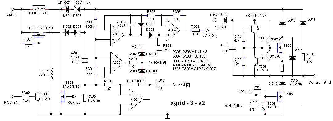
Figure 5.2 Extended grid bias supply
The idea behind the extended grid bias supply has already been discussed at some length on my “Lab Notebook Page where it was called, “bipolar grid bias supply” Figure 5.2 gives a first proposal towards a practical implementation. The positive voltage switch is a direct copy of the thoroughly tested high voltage switch used in the anode and screen supplies. For the current limit resistor an initial value of 2.7 ohm has been chosen since this is the same value used in the utracer 3 to limit the current to 250 mA.
In the present configuration the amplification of the current sense amplifier is set to A = 100/4.7 = 21.277. This means that the ADC input is 5 v for a voltage drop of 5/21.277 = 0.2347 V over the current sense resistor. With a current sense resistor value of 1.5 ohm this corresponds to a full scale maximum current of 156 mA, with a resolution of 165/1024 = 0.16 mA. The voltage divider is dimensioned in such a way that a voltage of 100 V maps to a voltage of 4.49 V at the input of the full-wave rectifier.
The anode and screen high-voltage supplies
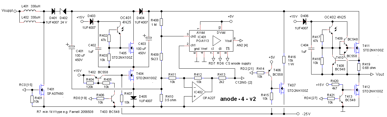
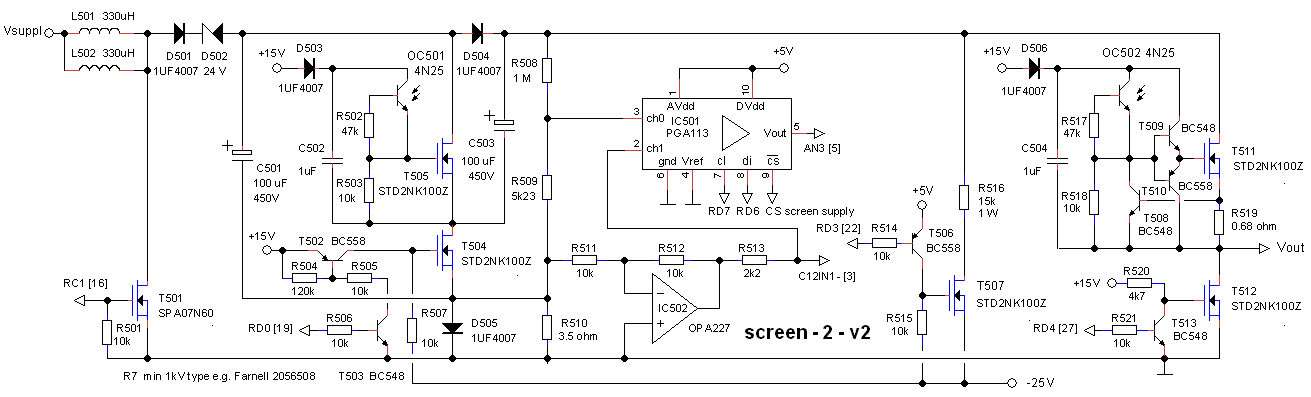
Figure 5.3 Anode and Screen high-voltage switch
The high-voltage supplies have already been extensively described in the previous sections. The uTracer 5 will contain two identical circuits one for the anode and one for the screen.
The CPU and power supplies
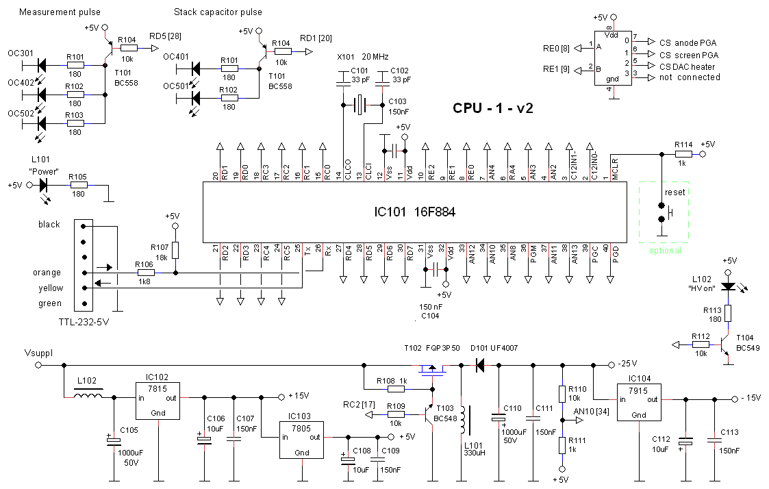
Figure 5.4 CPU and power supplies
Compared to the uTracer 3 the MAX232 RS232 interface has been dropped in favor of a TTL-232R-5V USB to RS232 converter cable from FDTI. These cables are not extremely cheap, but they work very reliable and eliminate the need for users to buy an additional USB->Serial converter. For more details read the entry on my Lab Notebook page.
The 16F876 that was used in the uTracer 3 is no longer recommended for new designs. A replacement suggested by microchip is the 16F884. Compared to the 16F876 the 16F884 has 2 more I/O’s, 14 ADC channels compared to 8, more RAM, more EEPROM and some additional features that are less important. Importantly it is almost pin and software compatible with its predecessor so that the uTracr 3 firmware skeleton can still be used.
Since in the uTracer 5 the three LEDs in the opto-couplers for the anode, screen and bipolar grid supply need to be driven simultaneously by the same PIC I/O, a buffer transistor has been added to make sure there is enough driver power. A small 2 to 4 decoder was used to decode the chip-select signals for the two PGA’s and the DAC. This solution, though it requires an additional SMD component, saves one scarce I/O pin. Should in the end turn out that there is an I/O pin left then this decoder can be omitted.
The DC power supply holds no mysteries, and is basically the same as the one used in the uTracer 3. Although the circuit uses less than 100 mA on the +5V supply, the 7805 in the uTracer 3 tends to become quite warm due to the large voltage drop across it, and therefore requires a small cooling element. For the uTracer 5 I have chosen to cascade the 7815 and the 7805 to reduce the voltage drop over the 7805 a bit. An alternative would have been to use a switching regulator instead of a 7805. However, I want the uTracer to be absolutely free from switching noise during the measurement, while on top of that the 5V supply is also used as reference for the AD converter, the amount of heat generated is quite acceptable anyway. The inverting boost converter for the negative supply voltage has been modified to generate -25 V. The voltage divider has been dimensioned in such a way that a voltage of -25 V maps to 2.272 V on the ADC input

A small personal souvenir of a fantastic holiday in the Yorkshire Dales: a panoramic view on Middleham from William’s Hill.
| to top of page | back to the uTracer homepage |
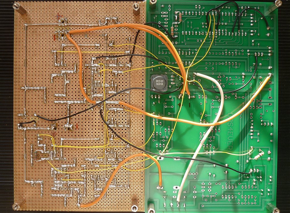
Time has come to make a first prototype version of the uTracer 5. At this point there were two options. Directly design a professional PCB for the circuit, or first construct a version on perf-board. Because the circuit is too big for a standard 10x16 (Eurocard) perf-board, I was very much tempted to go directly for the PCB version. However, that would require quite some time (and money) while it probably will need to be redesigned anyway. Personally I always prefer to first make a perf-board version. One way or the other it forces me to think about the optimal component placement, probably because it is very instructive to physically hold the components and move them around the board. Fortunately I could lay my hands on a large professional perf-board, so I decided to have a go at it!
Quite some time was spent on optimizing the layout of the high-voltage switches. The challenge here was that some parts of the circuit operate at very high voltages, up to 900 V, while other parts of the circuit are at low voltage directly connected to the micro-controller. To make things even more complicated, each switch uses quite a number of control and sense signals, and no less than 5 supply lines, including ground. Finally the circuit should be as small as possible.
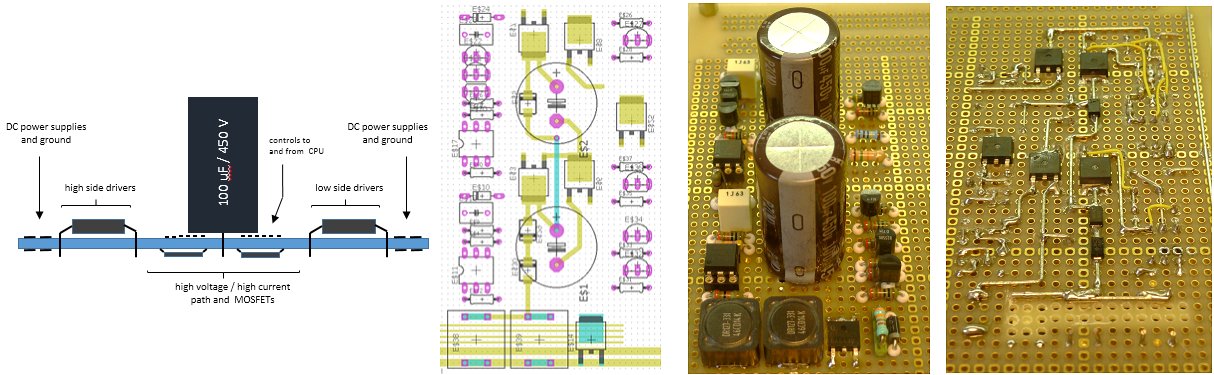
Figure 6.1 Component layout of the high voltage switches. Schematic cross-section and top-view (left) and perf-board implementation (right)
Figure 6.1 shows the circuit layout I arrived at. The schematic cross section and top view show that the circuit layout can be subdivided into three vertical columns. The left column contains the high-side driver circuits that operate at high voltages. They are the two “boots-strapped ”opto-coupler controlled MOSFET driver circuits. The middle column on the PCB contains on the bottom part of the PCB all the high current / high voltage wiring and all the high voltage MOSFETS. The top part of the PCB in that area is used to route all the control signals. They are kept at a safe distance from the high voltage driver circuits and the capacitor terminals. The right column, finally, contains the low-side driver circuits. The two photos on the right side show the perf-board implementation, without some of the control wiring. All in all a pretty small and compact piece of electronics.
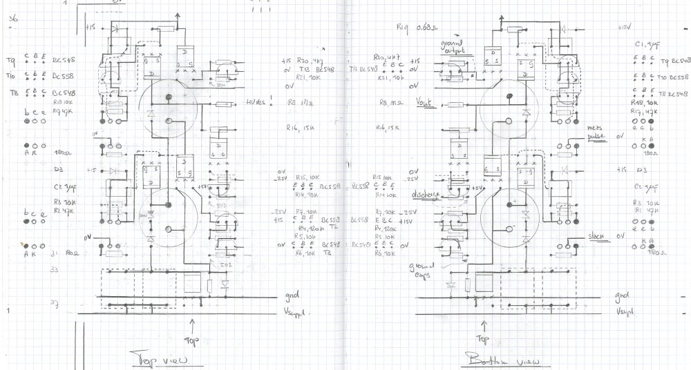
Figure 6.2 detailed planning of the layout on a 0.1 inch grid, front and backside.
Figire 6.2 gives an idea how the puzzle of component placement is solved on paper using pencil and eraser. Some people might find this a waste of time, but for me it is the sum mum of concentration and relaxation. There is nothing that can help clearing my mind as puzzling on an optimal layout and making a nice drawing. All parts of the circuit were planned in these detail, also to save time later on during the design of the real PCB.
Migrating from a 16F876 to a 16F884 processor
The 16F876 PIC processor that was used in the uTracer3 is becoming obsolete so that is why I decided to migrate to a more modern 16F884 PIC. The 16F884 is to a large extend compatible with the 16F876 and has some additional features. Features that are of interest to this project are: larger EEPROM memory, more RAM, and 14 AD inputs instead of 8. Unfortunately it is not possible to directly copy the firmware. Some registers have been renamed or moved to another memory bank. On top of that I still used my trusted DOS command line assembler that unfortunately does not support the 16F884. So it was time to move on to the newer windows MPASMWIN assembler.
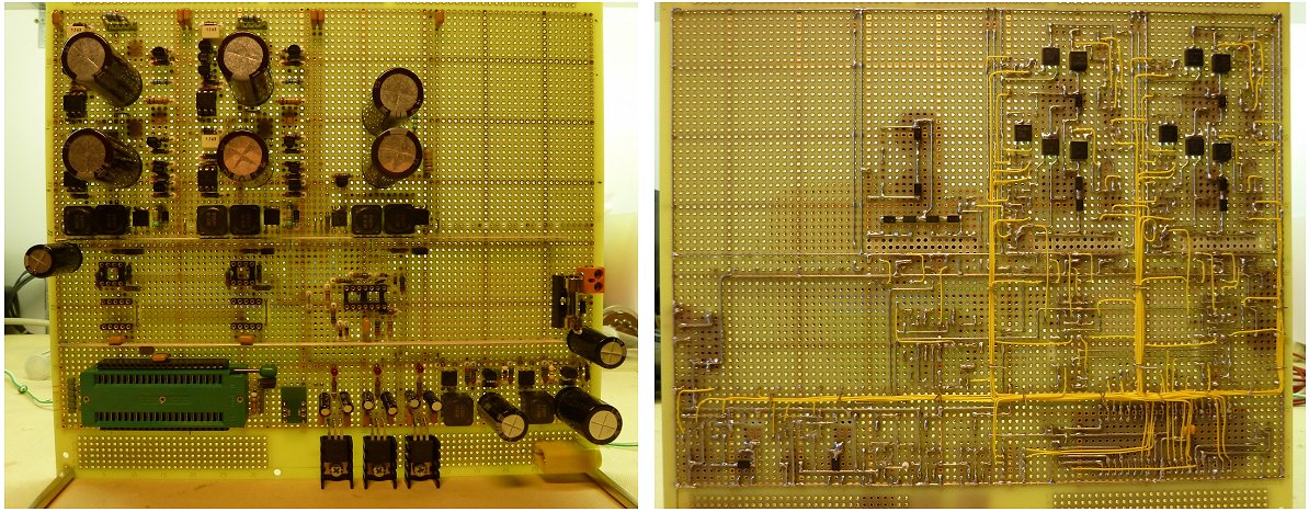
Figure 6.3 All individually tested circuit parts in place ready for the first stage of firmware testing.