 |
 |
 |
|
|
|
This prologue was written when this page was already well underway. I thought a few lines to introduce the meandering story line of this project page were needed. The uTracer7 project started as an exploration to find out if a 5000 V / 1A tracer for high power transmitter tubes using commonly available standard components is feasible.
Several ideas and concepts were explored. The first idea was still based on using capacitors as an energy storage element. The idea was discarded after a big bang, mainly for safety reasons. I then realized that inductors can also be used to store energy. They have the advantage that they cannot store energy after the power supply has been switched off. This led to some first experiments with a discarded fluorescent ballast inductor. Although encouraging, using a simple inductor still requires a not readily available high voltage switch.
YouTube movies of people doing crazy experiments with discarded microwave oven transformers (MOTs), led to the idea to us a MOT as the heart of uTracer7. First experiments were very promising, and at the writing of the prologue, it is now the main investigation path, with a prototype being developed.
As always, these pages primarily serve to document my own ideas and experiments. At this moment I have no idea if all this eventually will result in a kit. It will all depend on how the experiments will turn out, and the interest of potential users.
One of the nice things about the uTracer testimonial page is that I get a bit of an insight into the sort of tubes people want to trace. From the testimonials I received from people who built the uTracer6, I was astonished to see what “monster tubes” especially ham radio enthusiasts are using! Whereas I would have thought that the uTracer6 with its 1000 V and 1 A anode and screen supplies would cover all possible audio tubes, it appears that for most transmitter tubes the uTracer6 only covers a small part of their operation area. Not surprising, just like Dickens’ Oliver Twist, the proud owners of these tubes are asking “Please Sir, can I have some more!” I took it as a challenge to think about circuit concepts that will allow for full tracing of these monster tubes. It should be clear that, although I may do some experiments to test concepts, I have at this moment no plan whatsoever to make a uTracer kit for these very high scary voltages. Also because I do not want to be held liable should something go wrong!
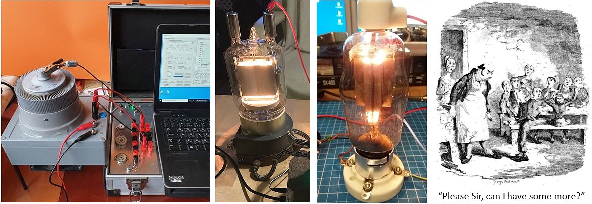
Figure 1.1 Some pictures from my testimonial page of the monster transmitter tubes being traced with the uTracer6.
Although with its 1000 V anode voltage the uTracer6 makes a good start, most people like Oliver Twist “would like to have some more”!
I made a small search on internet into the type of tubes ham radio amateurs use in their transmitter amplifiers. A small collection of them can be found in Fig. 1.2. It appears that anode voltages up to 5 kV at a current between 1 and 2 A would cover most tubes.
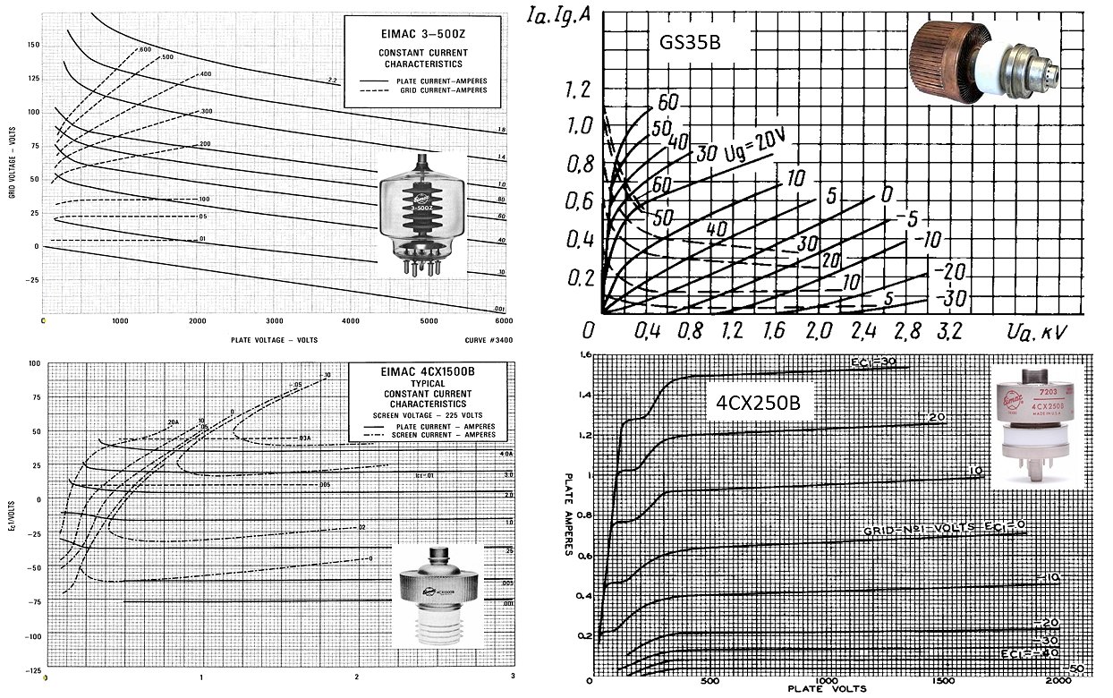
Figure 1.2 I made a small search on the internet into the type of tubes ham radio amateurs use in their transmitter amplifiers. It appears that anode voltages up to 5 kV at a current between 1 and 2 A would cover most tubes.
| to top of page | back to uTracer homepage |
My first idea was to revive the transformer idea again that I explored - and for various reasons abandoned - in the uTracer4 concept. The main attraction of that concept is its robustness. It appeared to be almost impossible to damage the circuit by a shorted output. Another attractive feature that I had in mind was to make the concept modular, so that to achieve higher currents more units could be placed in parallel. I looked at it with my colleague and transformer specialist Peter Bancken. We both agreed that that the concept could work, however, it would require a specially made transformer that had to combine a high output voltage with a very low spreading inductance, requirements that are difficult to combine.
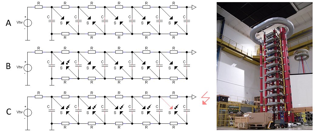
Figure 2.1 Principle of the Marx impulse generator (left); giant Marx generators (right) can produce pulses of millions of Volts and are used, for example, to test components in electricity distribution networks.
The idea of making something modular, where either higher currents or voltages can be obtained by switching units in parallel or in series somehow reminded me of the giant Marx impulse generator we had at the high voltage lab of my university in Eindhoven. From Wiki: a Marx generator is an electrical circuit first described by Erwin Otto Marx in 1924. Its purpose is to generate a high-voltage pulse from a low-voltage DC supply. Marx generators are used in high-energy physics experiments, as well as to simulate the effects of lightning on power-line gear and aviation equipment.
A Marx generates a high-voltage pulse by charging a number of capacitors in parallel, and then suddenly connecting them in series. Figure 2.1 shows the basic circuit. First, n capacitors C are charged in parallel to a voltage Vhv by a DC power supply through the resistors R (Fig. 2.1A). The spark gaps are used as switches, and have the voltage Vhv across them, but the gaps have a breakdown voltage greater than Vhv, so they all behave as open circuits while the capacitors charge. To create the output pulse, the first spark gap is caused to break down (Fig. 2.1B); the breakdown effectively shorts the gap, placing the first two capacitors in series, applying a voltage of about 2*Vhv across the second spark gap. Consequently, the second gap breaks down to add the third capacitor to the "stack", and the process continues to sequentially break down all the gaps (Fig. 2.1C). With all capacitors in series, an output pulse of n*Vhv is obtained at the last stage. The charge available is limited to the charge on the capacitors, so the output is a brief pulse as the capacitors discharge through the load. At some point, the spark gaps stop conducting, and the voltage supply begins charging the capacitors again.
Searching for “Marx generator” in Google will return many hits of both professional as well as amateur builders of Marx generators, obviously with the sole purpose to produce giant sparks. I especially like the YouTube video from ElectroBOOM!
A Marx uTracer?
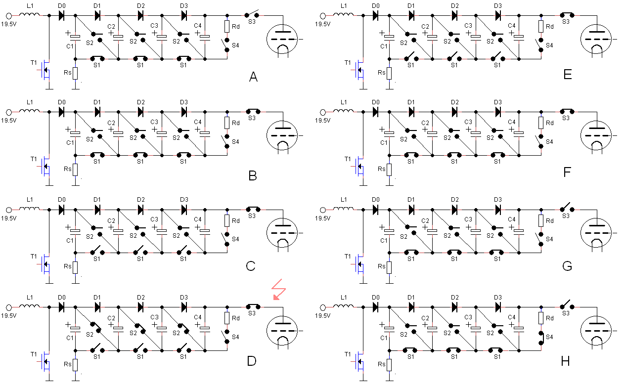
Figure 2.2 Schematical representation of the modular high voltage uTracer.
Since the uTracer also operates in a pulsed fashion, it seemed obvious to explore if the Marx concept can be adopted for a very high voltage uTracer. One very attractive aspect of the Marx generator is that during its operation both the resistors as well as the capacitors are never subjected to a voltage higher than the input voltage. This is very attractive since above 1500 V electronic components become very scarce and prohibitively expensive. A major difference with the standard Marx generator is that in the uTracer we need to interrupt the current after a fixed period of time of 1 ms, while in the Marx generator the current continues to run until the capacitors are so far discharged that the spark gaps open again. After some puzzling I came to a circuit that might do the trick.
The basic operation of the circuit is schematically explained in Fig. 2.2. At the center of the circuit in Fig. 2.2A we find capacitors C1 – C4, which obviously form the heart of the Marx generator. Note that on the bottom side of the ladder structure the resistors have been replaced by switches S1. On the top side of the ladder structure the resistors have been replaced by diodes. On the left side the ladder structure is not directly grounded, but connected to ground by a small series resistor that obviously will be used to measure the current during the measurement pulse. The DC voltage source in the traditional Marx generator has been replaced by a boost converter consisting of T1, L1 and D0. On the right side of the ladder switch S4 has been added to discharge the capacitors through Rd when needed. Finally, the spark gaps have been replaced by switches S2.
Operation:
(the letters refer to the corresponding figure in Fig. 2.2)
Towards a circuit
It will not come as a surprise that in the real circuit implementation that I have in mind the switches are replaced by transistors. The obvious challenge will be to find a simple way to control the transistors. Let’s first discuss voltages. To keep the total circuit as small as possible the voltage per ladder stage needs to be as high as possible. The SiC SCT2750NY transistors are rated at 1700 V, combined with an Rdson of 0.75 ohm and a continuous drain current of 6 A! For me they are the ideal candidate for all the high voltage transistors. To be on the safe side, the maximum voltage per ladder stage was set at 1500 V.
Figure 2.3 Simplified circuit diagram of the modular high voltage uTracer.
Figure 2.3 shows a simplified version of the actual circuit implementation. Going from left to right we first find the traditional booster configuration that is used in the other uTracers. To reach the 1500 V working voltage I plan to use three 330uF / 500V electrolytic capacitors in series. To ensure that the total voltage distributes evenly over the three capacitors, usually a resistive divider network is used. However, selecting the proper resistor values is tricky and besides this the resistors also dissipate. So here I plan to use Zener diodes that limit the voltage per capacitor to a value slightly above 500 V. When the voltage across a capacitor exceeds the maximum value the diode starts to conduct, forcing more current into the other caps.
Next, we move to the ladder sections. Transistors Ta obviously implement the switches S1 from Fig. 2.2. The gates of these transistors are controlled by a bus labelled “Open ladder.” This is an active-low signal. When it is 0 V, diodes Da block and the gates of the transistors are pulled low (with respect to their sources) by a resistor. When it rises to 20 V, first the most left transistor whose source is practically connected to ground via Rs will start to conduct. This will also pull the source of the second transistor Ta to ground so that also that transistor will turn on, etc. When the ladder is “erected,” and the different sections will be at a high potential, diodes Da will block, and the transistors Ta will be off. This means that some of the diodes Da will need to be able to block the maximum output voltage of the circuit! The high resistivity resistors Rl have been added to prevent the different branches of the ladder from “floating” when the transistors Ta are open.
When the ladder is in the “charging state,” the total equivalent high voltage capacitance for the circuit in Fig. 2.3 is: 3 x (330 uF / 3) = 330 uF. The first question now is: is it possible by using a simple boost converter, to charge a 330 uF capacitor to 1500 V in a reasonable time? I will come back to that question later. Apart from this, in the “erected state” all the capacitors are in series, and we end up with an equivalent capacitance of 330 uF / 9 = 37 uF. This is not so far off from the 50 uF in the uTracer6, but it is getting a bit on the small side. Up till now I have used the 10 ADC inputs of the microcontroller to sequentially poll the analog inputs. However, this inevitable means that there will be a time difference between the moment the voltage is measured and the moment the current is measured. In between these moments, the voltage of the capacitors may have dropped significantly. So for the first prototype I plan to use sample-and-holds, that capture both the voltage as well as the current at exactly the same moment.
The transistors Tb in Fig. 2.3 implement the switches S2 in Fig. 2.2. People who have studied the circuit diagram of the uTracer6 will undoubtably recognize the gate driver circuit for Tb. The circuit makes use of the fact that “bottom side” of the ladder will be at ground potential most of the time. In this state capacitor Cb will be charged to 20 V through diode Db. The capacitor acts as a little battery to power the gate driver circuit during the 1 ms measurement pulse. When transistors Tb are not conducting, their gates are tied to their sources by a resistor. The transistors are controlled by optocouplers that uses the charge stored in capacitors Cb. For the optocouplers I plan to use the affordable CNY66 that isolates voltages up to 13.5 kV.
On the right side of Fig. 2.3 we find the discharge circuit and the final output switch. In the discharge circuit transistor T2 fulfills two tasks. First, T2 is used to discharge capacitors Ca (if needed) through resistor Rd. At the same time T2 grounds capacitor Cb so that it can be charged. The output switch is identical to the ladder switches.
Figure 2.4 Detailed circuit diagram of the modular high voltage uTracer.
The open spaces in Fig. 2.3 already suggest that this is not the complete circuit. Correct! The way the gates of the transistors are driven in Fig. 2.3 is a bit too simple. The grid resistor that pulls the gate down unavoidably has a rather high impedance. Any fast transient on the drain can, through the drain-gate capacitance, pull the transistor into conduction with potentially disastrous consequences (read more about the so called dV/dt breakdown here). To tie the gates of the transistors firmly to ground when they should remain closed, totem pole buffers consisting of an emitter follower npn/pnp pair have been added. Actually, this small circuit is identical to the high-voltage switch driver already tested in the uTracer6.
Loose ends
Figure 2.5 Ta and Tb are protected by the Zener diodes across the electrolytic capacitors.
Although in principle the high voltage transistors in the circuit are never subjected to a voltage higher than the maximum voltage of a single ladder stage, it turned out that the Zener diodes used to guarantee the proper voltage distribution over the electrolytic capacitors also offer additional protection. When for example the voltage across Tb in Fig. 2.5a would become too high, the voltage is clamped by the stack of Zener diodes on the right side of the stage. Conversely, when the voltage across Ta becomes too high (Fig. 2.5b), the “body diode” of Tb opens and the voltage over Ta is clamped by the stack of Zener diodes over the capacitors on the left side of the circuit. The body diode is in circuit diagrams often omitted because in most circuits the drain always remains positive with respect to the source, however, here it is used to offer extra protection to the circuit. In the case of the SCT2750N the characteristics of the body diode are separately specified in the datasheet. It can handle a continuous current of 6 A and a peak current of 14 A.
Figure 2.6 Boost converter variations
It can easily be overlooked that also the inductor in the boost converter must be able to handle the full ladder stage voltage of 1500 V. From the extensive experience with the uTracer3 and 6 it is clear that the inductors from the DR127 series from Coiltronics / Eaton can perfectly handle voltages up to 500 V. By simply placing a number of inductors in series the maximum voltage can be distributed over the separate inductors. Since the induction voltage over the inductors is directly proportional to dI/dt, and since the same current flows through all the inductors, the voltage will always be evenly distributed. In the uTracer6 two inductors were used in series to be able to handle 1000 V. In this case three inductors of 100 uH can be used to roughly obtain the 330 uH to match the pulse length of the firmware controlled boost converters.
Mainly for my own administration a list of components I have in mind for the 5 kV uTracer:
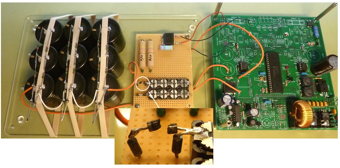
Figure 2.7 A first experiment to test the charging of a battery of 330uF / 500 V capacitors ended in a big bang! The capacitors were switched as three banks of three capacitors in series adding up to a voltage of 1500 V (@ 110 uF). The idea to use two UF4007 diodes in series in the boost converter (see Fig. 2.6) was apparently not a good idea as one of the diodes exploded with an enormous bang that made my ears whistle for the better part of an hour!
| to top of page | back to uTracer homepage |
While experimenting with the circuit of the 5 kV uTracer discussed in the previous section, something went wrong which left the high voltage reservoir capacitors partly charged. Fortunately, I thought of it, could discharge them safely, but had I forgotten to check them, I could have been in for a very nasty surprise! Not wanting to rely on my alertness to continuously check the status of the capacitors during experiments, I felt the need for a circuit that will warn me if the capacitors are charged to a dangerous voltage. It resulted in a simple circuit that might be of interest to other uTracer owners who want to add some safety to their uTracer builds.
Below the design requirements for the lifesaver:
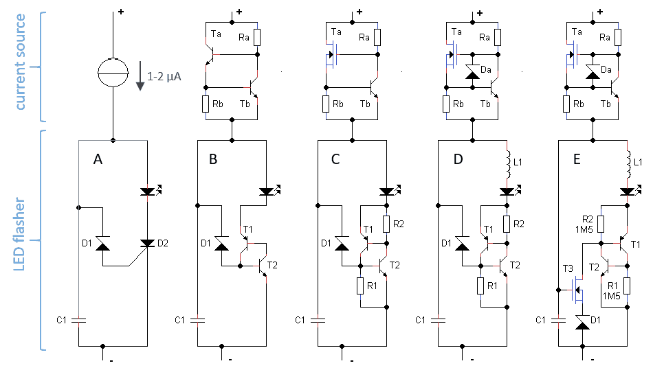
Figure 3.1 The conception of the lifesaver step-by-step.
Obviously a circuit that makes a current of a few micro-amps flash an LED will need to consist of a capacitor and some form of threshold detector with switch that discharges the capacitor through the LED. The basic idea of the circuit is shown in Fig. 3.1A. It consists of two parts, a current source that limits the current drawn by the circuit to a few micro-amps and makes it independent of the input voltage, and the flasher circuit.
Let’s first concentrate on the flasher circuit. The simple idea was to let the current charge capacitor C1 until the voltage over the capacitor becomes so high that zenerdiode D1 starts to conduct thereby triggering thyristor D2. The thyristor discharges the capacitor through the LED until the capacitor is discharged, and the thyristor comes out of conduction. The low power thyristor can conveniently be implemented by a pnp transistor tightly coupled to an npn transistor Fig. 3.1B (also have a look here). The problem with this circuit is that the gain of common transistors is so high that the smallest noise in the circuit will trigger the thyristor at unpredictable moments. The problem is easily solved by connecting two high value resistors over the emitter-base junctions of the two transistors Fig. 3.1C. This will effectively kill the gain of the transistors at low currents, making it a reliable simulated thyristor.
Disappointingly, the circuit still did’t work as expected. The capacitor charged as it should, and when the capacitor voltage increased beyond the voltage of the zener diode the thyristor fired as expected flashing the LED and at the same time discharging C1. However, instead of starting the cycle all over again, the circuit froze at the point where the current supplied to the circuit would just keep the thyristor conducting. The solution to this was to include a small inductor in series with the LED (see Fig. 3.1D). The inductor in combination with the capacitor forms a resonant circuit that gives the circuit a flywheel character whereby the current is really pushed to zero so that thyristor comes out of conduction.
The circuit of Fig. 3.1D worked well, but only for reasonable currents. For currents in the few micro-amp range the circuit again froze in a state where the current needed to trigger the thyristor was larger than the current supplied to the circuit. So for this circuit to work, the current drawn during the charging of the capacitor should be an order of magnitude or more less than the supply current. This was easily remedied by the addition of MOSFET T3 (Fig. 3.1E). With zenerdiode D1 in series with the gate, T3 will only start to conduct when the gate voltage exceeds its threshold voltage plus the zenerdiode voltage, while the gate of T3 of course draws zero current. Note that in this case the thyristor is not trigger by pulling the base of T2 up, but by pulling the base of T1 down. This really did the trick and the circuit now works very satisfactory even for currents well below 1 uA.
Before attentive readers start writing me emails, I know that there are special energy scavenging ICs like the LTC3588 or the S6AE101A, but that would have been half so much fun, and they are quite expensive anyway.
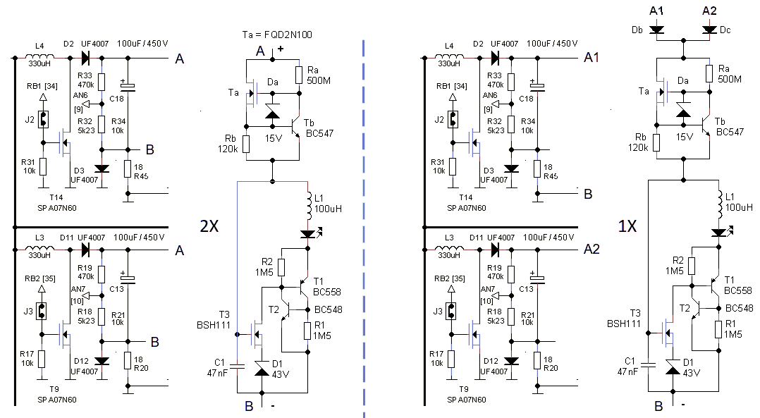
Figure 3.2 Left, connection of the lifesaver circuit to the uTracer in case each capacitor has its own lifesaver circuit. Right, connection if one circuit is used to monitor both capacitors.
What remains to be discussed is the current source. For that I used a circuit that most of you will recognize as the current limiting circuit in many simple power supplies. It consists of transistor Ta that is basically pulled into conduction by resistor Ra (topside of Fig. 3.1B). Rb senses the current and as soon as the current exceeds approximately 0.8 V, transistor Tb will start to conduct thereby cutting off Ta. This will stabilize the current at a value determined by Rb. I used a MOSFET for Ta since I didn’t want to bother with a base current and I had some lying around anyway. Diode Da protects the gate of the MOSFET against an excessive gate voltage should anything go wrong.
In Fig. 3.2 some component values have been added to the circuit. For the 1000 V version of the circuit an FQD2N100 or STD2NK100 or equivalent can be used for Ta. If you want to use the lifesaver for the uTracer3 obviously a transistor with a lower breakdown voltage can be selected. Resistor Ra should be as high as possible since the current through this resistor adds to the total current making the current source voltage dependent. I used a 500 Mohm resistor from Murata (available from Mouser). The MHR_SA series of resistors from Murata offers resistors up to 1 Gohm with up to 20 kV rating for a very reasonable price. For the inductor I used a 100 uH axial type, the value is not particularly critical. I don’t know where I got this particular inductor from, but I guess that any readily available inductor like this one available from Mouser will do. For the LED a high intensity type gives the best results. I used a 3500 mcd white VAOL-3GWY4 from VCC.
Figure 3.2 shows how the lifesaver can be connected to the uTracer. If you plan to use a seperate lifesaver circuit for each of the two high voltage electrolytic capacitors the circuit can be connected directly over each of the capacitors (Fig. 3.2A). In this way, the current used by the circuit is not flowing through the current sense resistor and so is not detected at all. It is also possible to use one circuit for both capacitors by using two diodes in an “or” configuration (Fig. 3.2B). Obviously, in that case it is unknown which of the two capacitors (or both) is charged.
The (rather poor) movie below shows the circuit in action on breadboard. I am not going to bother designing a PCB for it, but will simply transfer it to perfboard(s). It is fun to experiment with the circuit. Increasing the value of C1 will increase the intensity of the flash but reduce the flash frequency. This can be compensated for by increasing the current by lowering the value of Rb. The voltage at which the circuit starts flashing can be adjusted by changing the breakdown voltage of the zener diode, which will also effect the brightness of the flash etc etc. In the test setup shown in the movie below I connected a piezo speaker in parallel with the LED to also give an acoustic feedback signal. Perhaps a small normal speaker in series with the LED will also work and provide enough inductance so that L1 is not needed? In short, have fun but be careful with high voltages!
| to top of page | back to uTracer homepage |
The first experiments with the Marx generator inspired idea for a very high voltage uTracer turned out to be rather a disappointment. The first experiments to see if it is feasible to charge a battery of electrolytic capacitors with a simple boost converter ended literally with a big bang when a UF4007 diode in one of the boost converter branches exploded. Although I still think there is some merit in the concept, I came to the following thoughts / conclusions.
First, very high voltage capacitors with any significant capacitance are very scarce. In practice 500 V rated electrolytic capacitors are at the upper range of what is commercially available. So, to get to a higher voltage, stacking (placing in series) of capacitors is the only option. This is not straightforward. Special measures are needed to ensure that capacitors in series are charged equally, even in case they have small differences in leakage currents. On top of that the total capacitance of the stack decreases inversely proportional to the number of capacitors stacked.
Secondly, if we want to go to higher voltages and currents, it becomes almost unavoidable to go to shorter measurement pulses. In the first place just to reduce the volume (and cost) of the storage capacitors, but in the second place also from a safety point of view. In the capacitor bank shown in Fig. 2.7 I had 9 capacitors of 330 uF all charged to 500 V. Such a monster can kill you if you are unlucky! Going to shorter measurement pulses automatically means that we cannot simply successively readout the analog signals with the single AD converter of the PIC anymore, but that we will need sample-and-holds, perhaps even in combination with multiple AD converters to capture voltages and currents accurately in the same moment of time.
Turning things around
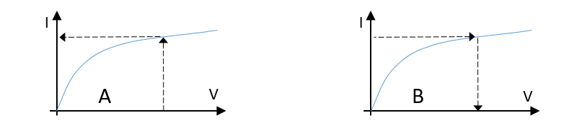
Figure 4.1 Instead of applying a voltage and measuring the resultant current (A), it is just as well possible to force a current and measure the resultant voltage (B).
My normal work, and the demand for uTracer kits (and the associated desperate searching for the necessary components) kept me pretty busy the past months. Nevertheless, the thoughts about the 5 kV / 1 A version are never far away, especially not at night. At one of these moments it occurred to me that it might perhaps be advantageous to turn things around, and not use a capacitor to store the energy for the measurement pulse, but an inductor! A capacitor stores energy in the form of charge that at the terminals is available as a voltage that, connected to a load, will result in a current. An inductor stores energy in the form of magnetization that at the terminals is available as a current that, connected to a load, will result in a voltage (Fig. 4.1).
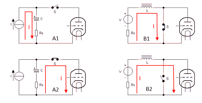
Figure 4.2 Left (A1&A2), basic working of the uTracer3 & 6. Right (B1&B2) principal idea of the “turned around” concept.
This arrangement has several advantages:
Already from the onset a few disadvantages of the new circuit are clear, and I am pretty sure that going along I will discover a few more:
A first shot
Somehow it occurred to me that the inductive ballasts that were (are) used in fluorescent lamps might be a good candidate inductor for the first experiments. They have a significant inductance in the order of 1 H and are designed to sustain a voltage well in excess of 1000 V. Unfortunately, I didn’t have any lying around, but fortunately my colleague Peter Blanken just replaced all the fluorescent lights in his house with LED lights and he was so kind to donate four of them to the cause of tube tester research.
It is very simple to determine the inductance of this type of large inductors. First, simply measure the DC resistance Rdc. Then connect the inductor to an AC voltage. I my case I used a 20 V transformer. Measure the voltage across the inductor terminals and the current flowing through the inductor. This yields the total impedance of the inductor Z = V/I. The inductance now follows from L = (Z-Rdc)/(2*pi*freq). The inductors I had were all designed for 36-40 W / 230 V fluorescent lamps, and despite the fact that all four of them came from different manufacturers, they all had a DC resistance close to 43 ohm, and an inductance around 1.3 H. Apart from the DC resistance and the inductance the saturation current is an important parameter. More about that in the next section.
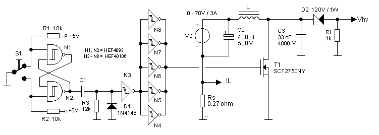
Figure 4.3 Circuit diagram of the test circuit.
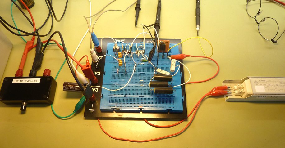
Figure 4.4 Breadboard setup.
Just to get a first hands-on feeling on how the circuit with such a ballast inductor would function, I breadboarded a quick and dirty test setup (Fig. 4.3 and 4.4). The circuit consists of a simple debounced pushbutton, and a one-shot. The pulse width of the one-shot can be crudely set by changing capacitor C1. The pulse from the one-shot drives the gate of a SCT2750 SiC MESFET. This SiC monster transistor combines a breakdown voltage of 1700 V with an on-resistance of 0.75 ohm. It is the same transistor that is used in the boost converter of the uTracer6. The circuit around the inductor is powered by a floating, well decoupled power supply. The power supply is connected to ground via a small current sense resistor that is used to monitor the current through the inductor. Note that in this arrangement the current will cause a negative voltage drop over the resistor with respect to ground!
Capacitor C3 is added to broaden the width of the high-voltage pulse. When the inductor is “charged,” and T1 is opened part of the current will charge C3. When the voltage has reached its maximum the current through C3 will reverse, and it will start dumping its charge into the load. Of course, this somewhat reduces the output voltage, but it makes life for the sample-and-hold circuits much easier. There is another benefit! With a small series resistance in the ground connection of C3 the current reversal at the maximum output voltage can be detected. This can be used to trigger the sample-and-hold circuits. Zener diode D2 is necessary to ensure that during the off-state, and the inductor charging phase the current though the load is zero. The breakdown voltage of the Zener diode must be higher than the power supply voltage Vb. In this experiment I had a 120V / 1W diode lying around that I used. For the load I used a heavy duty 1k / 5W power resistor. At 1 A current the output voltage will be 1000 V what I consider to be on the safe side for the inductor.
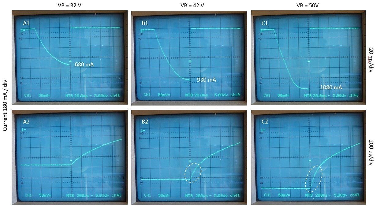
Figure 4.5 “Charging” the inductor with three different voltages. The current is measured by measuring the voltage drop over resistor Rs. Because this voltage drop is measured with respect to ground it has a negative sign. The small triangle indicates the trigger point which coincides with the moment T1 is opened. In the top row measurements the time base it set to 20 ms to register the charging process. In the bottom row measurements the time base is set to 200 us to zoom in to the discharging of the inductor.
The first thing to have a look at is the saturation behavior of the inductor. The simplest way to do that is to apply a constant voltage to the inductor and monitor the current. For a perfect inductor the current will increase linear with time (∆I = (V/L)* ∆t) until the point of saturation. At that point all the magnetic domains in the iron core of the inductor will be completely aligned with the magnetic field so that they cannot contribute to the inductance anymore with a further current increase. Basically, from that point onward, the core of the inductor is out of the equation, and what remains is an air inductor with a much smaller inductance resulting in a sharp increase in current.
In our inductor the situation is a bit more complex because of the relatively high series resistance of the inductor, which tends to obscure the saturation behavior. The snapshots in Fig. 2.5 show the current through the inductor as a function of time as measured over series resistance Rs. Because of the direction of the current this voltage drop is negative with respect to ground. With a maximum voltage of my power supply of 50 V, it takes about 70 ms to charge the inductor to approximately 1 A. The three columns Fig. 2.5 show measurements at supply voltages 32 V, 42 V and 50 V respectively. The two rows represent the same measurements, but at a different timescale. Note that none of the top row measurements shows the sharp increase in current we would expect in case of saturation. For column A I am pretty sure the core has not saturated yet. In Fig. B1 we clearly see the current leveling off. I am convinced the core starts to saturate at this point. From that point onwards, the current remains constant, and is completely determined by the supply voltage and the series resistance. Note that Vb / Rs = 42 / 44 = 0.95 A ≈ 0.930 A. More telling are the zoomed-in Figs. B2 and C2. The curves left to the trigger point (center) appear to be constant, because we are now looking at a 100x smaller time scale. To the right of the center we see the discharging phase of the inductor. Note that the first part of this discharge in Figs. B2 and C2 progresses much faster (encircled) than in remaining part of the curve. I assume that at that moment the core is still saturated, and we only see the small inductance of the air coil resulting in a much smaller time constant. At a certain point, basically corresponding to the current level of Fig. A2, the inductor comes out of saturation and the discharging continues at a much slower pace.
In short, our ballast inductor can certainly be used to a current of ≈ 700 mA, but as we will see in the following even 1 A is certainly possible.
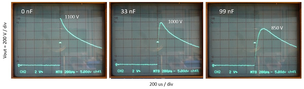
Figure 4.6 Voltage at the drain of T1 for three different values of C3.
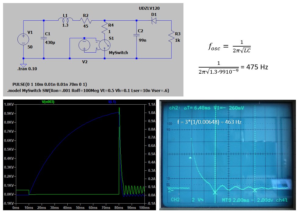
Figure 4.7 LTspice simulation of the basic circuit. Click here to download the LTspice input file.
Figure 4.7 shows an LTspice simulation of the circuit. In the simulation T1 is replaced by an ideal switch. Apart from the series resistance of the inductor no losses have been considered, and also the saturation of the inductor is not modeled. Despite this, the simulated version of the circuit shows a good agreement with the measurements. The simulations revealed quite pronounced oscillations that occur after the voltage has dropped to the level when the Zener diode stops conducting. Also, the measurements show the oscillations with a measured frequency of approximately 463 Hz, which corresponds perfectly with the resonance circuit formed by inductor L and C3 (L1 and C2 in the simulation).
Conclusions and outlook
Time for some conclusions and some ideas on if and how to continue:

Figure 4.8 My colleagues Bert and Peter. Both men have worked at Philips Research their whole working careers and are experts in power and analog electronics, the best possible sparing partners to discuss uTracer ideas.
The progress on the 5 kV / 1A uTracer is going much slower than I had hoped for. This is partly due to my normal work, but certainly also due to the success of the uTracer3 and uTracer6! At the end of the year, I hope to (partially?) retire so that I finally will have the time to work on it seriously. However, at the moment my wife and I are enjoying two weeks of holidays at my favorite part of the Dutch coast, Zeeuws Vlaanderen. The weather in Holland can be quite unpredictable, however, this time we are very lucky and blessed with excellent weather. We have rented a small cottage near the tiny village of Retranchement, which is just as the whole region here rich with history. The mornings here are spend on biking to beautiful destinations as Brugge (Bruges) , Knokke , or Middelburg, while the afternoons offer plenty of time to think about and ponder on the high voltage uTracer project.
The return of the transformer
Back to tube testing again. In the previous section I argued the use of an inductor as an energy storage element for the 5 kV uTracer. The main arguments where an automatic conversion of current into high voltage, and safety. Right from the beginning my colleagues Bert and Peter, with whom I always discuss many uTracer ideas (see Fig. 4.8), had suggested the use of a transformer instead of a simple inductor, and they are very right of course! The two main advantages of a transformer are first that at the primary side, where you “inject” the energy into the magnetic field, a low resistivity winding and hence a low driving voltage can be used. Secondly, during the flyback, the very high output voltage is transformed down to a moderate voltage at the primary side, thereby eliminating the need for a beautiful, but rather cumbersome line output tube.
However, the problem with transformers is always availability. Transformers, especially “specialties,” are notorious difficult components for hobbyist to get their hands on. By using a single, what I thought to be commonly available inductor in the form of a fluorescent ballast inductor, I had hoped to solve that problem. However, it appears that electronic ballasts have already replaced so much old magnetic ballast, that they are also rapidly becoming an obscure component! This dilemma, to be honest, was also one of the reasons for the delay in the uTracer7 project.
Then I came across a YouTube video of somebody who used an old Microwave Oven Transformer (MOT) to generate enormous sparks. I discovered that there is a whole society of people scavenging old MOTs to do life threatening experiments with no other apparent goal than to generate record length sparks. A bit to my shame, I have to confess that I didn’t have a clue about the high voltage electronics inside a microwave oven. It all appears to be pretty straightforward, and there are some very interesting video’s explaining it better than I can do in words here. At the heart of circuit is, next the the magnetron itself, a beautiful “specialty” transformer with a very “sturdy” 230 V primary winding (120 V in some parts of the world), and a 2500-3000 V secondary winding. Next to that, there is a third winding, usually only a few turns, to power the filament of the magnetron. Since the transformer has to generate in excess of a kilo Watt of power, the transformer is huge and the windings have low series resistances. And, the best thing is that there are millions of them in circulation, so it is not to difficult for anybody to salvage one from an old discarded microwave oven!
The discovery of the MOT brought new life into the project. Would this be a suitable magnetic storage element for the uTracer7?
Size matters!
It took a few weeks to get my hands on a discarded microwave oven and scavenge the transformer. The thing to notice was that it is absolutely huge (and heavy)! What is furthermore striking is the very rough way it is made. Apparently, everything is aimed at producing these transformers at absolute minimum costs. But as we will see, this also has its advantages!

Like many other transformers, the MOT has a E-I type core, however, in most transformers the E and I parts are alternated top-bottom to eliminate the chance for an air gap. In the MOT all the E laminates and I laminates are stacked separately, and the two parts are just welded together. For me that has the great advantage that it is rather simple to separate the parts and introduce an air gap that we will probably need. Browsing the web, I found a few other people who went along the same path to turn the MOT into a choke for tube amplifier power supplies etc.
The transformer is provided with two what are called “magnetic shunts.” These are small steel blocks of metal inserted in between the primary and secondary windings. The purpose of these blocks is to tap some of the magnetic field lines from the main core so that they only enclose the primary or the secondary windings. This will reduce the coupling between the two windings and introduce leakage inductance. Leakage inductance can be thought of a sperate inductance in series with the primary (or secondary) winding of the transformer (have a look here). It is a simple trick to limit the currents in an overload or short circuit situation. We absolutely don’t need then, and fortunately they it is easy to removed them.
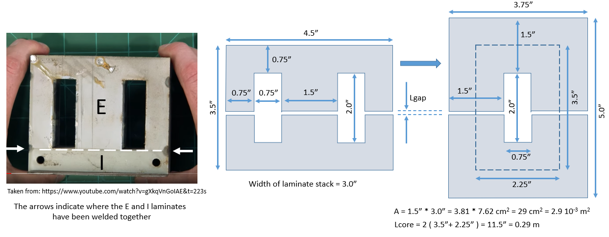
Figure 5.1 Estimation of the microwave transformer dimensions during my holidays from the YouTube video by Chris Boden.
I got the transformer just before the above mentioned holidays, so I only had time to do some basic measurements. On first inspection, I found a primary resistance of 2.1 ohm, a secondary resistance of 156 ohm and ratio of turns of 11. I didn’t have the time to measure any inductances or the saturation behavior, important parameters to determine if we can use a MOT for the uTracer7. Fortunately, these parameters can be calculated with reasonable accuracy. To do that the dimensions of the transformer need to be known. Unfortunately, I forgot to measure them before going on holidays, but fortunately Chris Boden from the YouTube channel Chaotic Good was so kind as to dissect an MOT on a cutting mat with inch markings from which it was quite easy to estimate the dimensions of the transformer (Fig. 5.1). Again, this will only be a first indication, measurements will provide the definitive answer. I give the calculations here mainly for my own documentation.
The calculation of the magnetic flux density and inductance is rather straightforward, and for anybody who wants to refresh their minds on the topic I recommend this excellent video on the YouTube Applied Science channel. In the calculations here I will already assume that we probably will need to introduce an air gap in the metal core. Without it, the core will most likely saturate well before we can store the amount of energy that we need. However, the introduction of an air gap will also strongly reduce the inductance. Our quest is to see if we can tune the airgap in such a way that we find a combination of L and Isat, which results in the storage of the necessary amount of energy ( 0.5*L*Isat^2).
We start by calculating the “magnetic resistance,” or better, the Reluctance R. To make this a bit simpler, I converted the magnetic circuit into a simpler and equivalent topology (Fig. 5.1 right two drawings). Purist will object that in reality the magnetic path in the core is somewhat shorter, however, since both the inductance and the magnetic flux density will be highly determined by the airgap anyway, so I neglect that for a moment. Furthermore, I assumed a relative permeability of 1500 for the steel core.
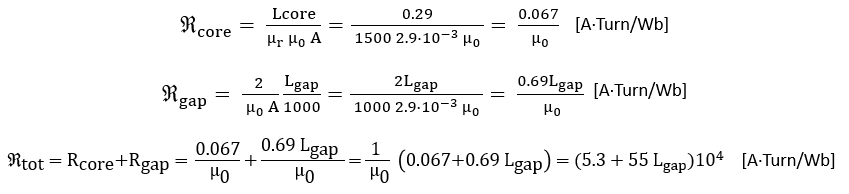
To calculate the magnetomotoric force that is driving the magnetic circuits we need the number of turns at the primary side. The cross sectional picture above is from a MOT intended for the 120 V US market. The number of primary turns can be counted and amount to exactly 100. Sor for a 230 V transformer I estimate 200 turns:

The total magnetic flux in the circuit now follows from:
The inductance is now the total enclosed flux by the windings per unit current:
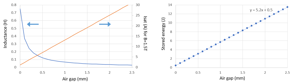
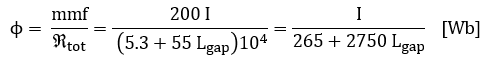
Figure 5.2 Left: calculated inductance and primary current at a saturation flux density of 1.5 T for a 240 V microwave oven transformer. Right: maximum amount of energy that can be stored before saturation as a function of air gap.
The basic circuit
To get an idea if a microwave transformer (MOT) can be up to the job, lets first have a look at the most basic circuit implementation, and for the moment neglect all losses and secondary effects. The first and most basic question is, considering an ideal MOT, can we store enough energy in the microwave transformer to generate a 5 kV pulse at a current of 1 A and with a reasonable width?
A “back of the envelope” approach is to assume that the output pulse is rectangular, say with a length of 200 us and with an amplitude of 5 kV @ 1 A. The instantaneous power dissipation is then P = 5000 V * 1 A = 5000 Watt. During 200 us this amounts to an energy of 5000 W * 0.0002 s = 1 J. So if there are no losses in the circuit, we at least have to be able to store at least 1 J of energy in the transformer to make this idea work. A more precise answer can be obtained with a simple circuit simulation using LTspice. Figure 5.3 shows the most basic version of the circuit. For the moment, all components are ideal and without losses.
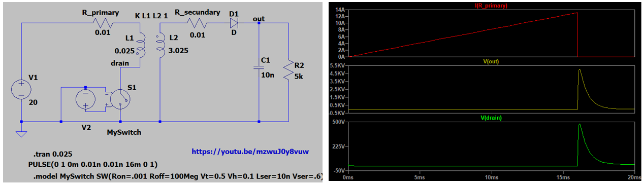
Figure 5.3 The circuit in its most rudimentary form, neglecting losses and assuming a perfectly coupled transformer.
Download the LTspice circuit description file here.
At the heart of the circuit we find the transformer. The simplest way to model a transformer in LTspice is to couple two inductors with the “K” statement (have a look at the YouTube tutorial by Linear Technology). Using this model, if the ratio of turns prim : sec is 1 : Nturns, the secondary inductance equals Lprim*Nturns^2. So if the ratio of turns is 11, as in our case, and for the moment we assume a primary inductance of 25 mH, the secondary inductance will be 0.025*11^2 = 0.025*121 = 3.025 H.
The circuit itself is straightforward. Download the LTspice circuit description file here. Like the uTracer3 and 6 I assume that the circuit is powered by an old laptop power supply of approximately 20 V. At the start of the simulation the voltage-controlled switch is closed so that the power supply is directly connected to the primary side of the transformer. As a result, the current thought the magnetization inductance with increase linearly (Fig. 5.3 right). This will induce a voltage of -20*11 = -220 V at the secondary side that is blocked by diode D1. After a certain time, in this example 16 ms, the switch opens. Since the magnetic flux cannot change instantaneously, a current is induced in the secondary winding that will flow through D1, transferring all the magnetic energy to C1 and R2, resulting in a high voltage pulse at the output. At the same time the voltage on the open switch at the primary side swings to 5 kV / 11 = 450 V.
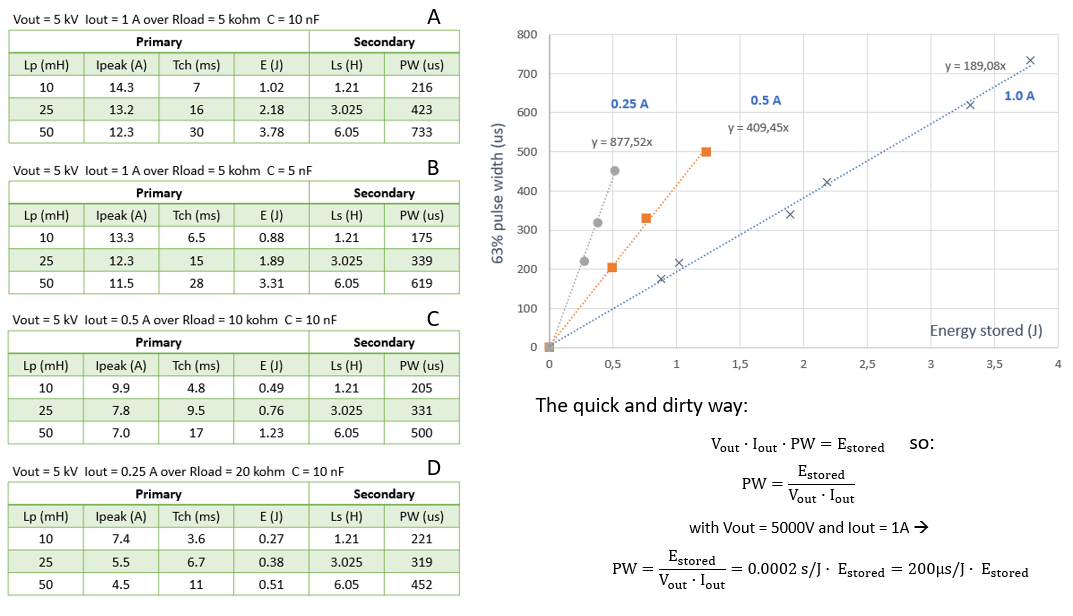
Figure 5.4 The rather complicated table on the left shows for the idealized circuit shown in Fig. 5.3 how much it takes to charge the primary inductance of the transformer for a 5 kV output pulse in a resistive load with values corresponding to peak output currents of 1 A, 0.5 A, and 0.25 A. The calculations are done for three different inductance values: 10, 25 and 50 mH. The output pulse width at 63% of the maximum output voltage is recorded and in the graph plotted against the energy stored in the inductor.
Not knowing a priori at what inductances for the transformer we will arrive at, I made a best guess and did simulations for Lprim = 10, 25 and 50 mH, corresponding to Lsec = 1.21, 3.025 and 6.05 H. In all simulations the “charging time” Tch, that is the on-time of the switch, was adjusted so that a peak output voltage of 5 kV was reached. In the Figs. 5.4 A&B a load resistor of 5 kOhm was used, so that 5 kV output voltage corresponds to 1 A output current. The width of the pulse at the output was determined at 63% of 5 kV so 3.12 kV.
As an example, using a 10 nF capacitor and a primary inductance of 25 mH, we need a peak primary current of 13.2 A, which at a supply voltage is reached after a charging time of 16 ms. At that moment 2.18 J is stored in the transformer, and the pulse width at the output is a comfortable 423 us.
Figs. 5.3 C&D show the same calculations, but now for 0.5 A and 0.25 A output current respectively. The graph in Fig. 5.3 shows for these simulations the pulse width as a function of the energy stored in the transformer. Note that for a given output current the points are neatly on a straight line, with a slope exactly corresponding the simple “quick and dirty” calculation!
Decapitating an MOT
In the meantime, the holidays are long over, and my regular job and the assembly of two brand new sets of uTracer kits have kept me busy. I must confess that being busy was not the only reason why the first experiments with an MOT were delayed a bit. Not being a natural mechanic, it took some courage to decapitate my MOT as I was not sure how to tackle it. Eventually a colleague suggested using an Dremel EZ lock cut-off wheel. That worked very well. It is important to remember that every bit of material that is removed will reduce the effective coil area, resulting in a less favorable inductance-saturation trade-off.
I found that the best way to go at it, is to first mark with a Sharpy or another marker the line where to cut the weld. The next step is to follow the line with the grinding tool, making a first guidance trench into the weld. It is important to alternatingly work on both sides of the transformer, because only when at both sides of the transformer the welds are completely removed, you will know that the cut has been deep enough. I had the impression that the heat of the cut-off wheel also tended to “melt” the two sides of the core together. In the end it took a few blows with a hammer to separate the two halves. After the two halves were separated, I noticed that the cut at the two ends tended to be deeper than in the middle, which not surprising if you are moving the wheel back and forth over the cut, but something to keep in mind.
A microwave transformer contains two magnetic shunts. There shunts are metal bars that are inserted in between the primary and secondary windings in such a way that they divert some of the magnetic flux away from the main core so that it only flows through the primary (or secondary) windings. This increases the leakage inductance of the transformer, which can be modelled as a separate inductor in series with the transformer. Normally, leakage inductance is unwanted and should be minimized as much as possible, however, in some cases it helps to make the transformer more resistant against short circuits as it acts pretty much in the same way as a magnetic ballast coil in fluorescent lighting. In our case we absolutely don’t need it, and fortunately the shunts can be easily removed by gently tapping on them with a hammer using a thin punch. Finally, the filament winding is removed.
Very instructive is the site from Guy Fernando, who modified a MOT for power electronics projects, and the site from Henry Hurrass, who turned an old MOT into a heavy duty plate choke.
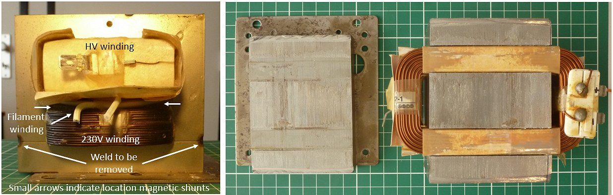
Figure 5.5 Left: face view of the MOT before decapitation. Right: the two halves of the MOT on a 1 cm grid.
First measurements
As a first model for the transformer, I used the equivalent circuit shown in Fig. 5.6. This model includes the resistances of the windings, the magnetization inductance Lm, and the leakage inductance Ls, but it does not model core saturation or losses. Interested readers are referred to my page on the uTracer4.
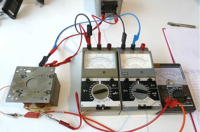
The method to extract the component values in the equivalent circuit is straightforward, and also explained on the uTracer4 blog. The resistance values can simply be found using a multimeter, although for the primary winding a four point measurement was used. The sum of the magnetization and the leakage inductances and the ratio of turns were found by connecting the primary side of the transformer to the 10 V output of a normal 50 Hz mains transformer and measuring the current through, and the voltage over the primary turns of the MOT, while at the same time the voltage at the secondary side was measured (see figure to the right). The leakage inductance was measured at the primary side of the MOT with the high voltage winding shortened using my good old BN6100 Rohde & Schwartz inductance meter (1972 and still going strong). Finally, the magnetization inductance was calculated by subtracting the leakage inductance from the already measured sum of the two.
The table in Fig. 5.6 lists Lm and Ls as a function of the air gap height, which was varied by inserting 250 um thick paper index cards between the two core halves. It made little difference to the measured inductance values whether the two halves were pressed together or not. The weight of the transformer is enough to stabilize the values. However, the transformer made a distinct 100 Hz hum, that almost disappeared when the core halves were firmly pressed together. Since sound represents energy, and thus losses, I suspect that pressing the halves together will reduce core losses.
The graph in Fig. 5.6 reproduces the calculated inductance of Fig. 5.2, and the values of the measured magnetization inductance (dots) have been added. It is surprising how well the relatively simple inductance calculation predict the measured values. This gives some confidence that although the saturation current could not be measured at this point, the calculations also predict this parameter with reasonable accuracy.
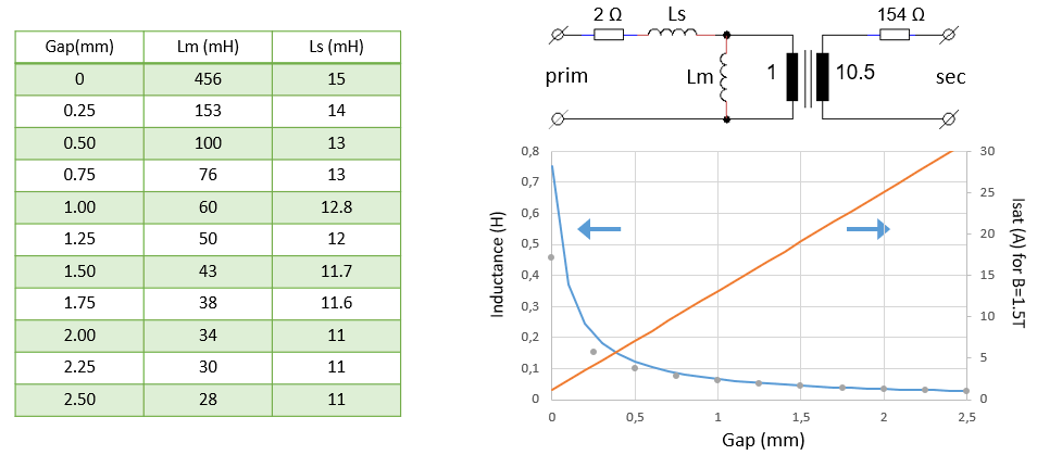
Figure 5.6 Table: measured magnetization and leakage inductances as function of air gap height. Graph: measured magnetization inductance (dots) compared to the calculated inductance.
Figure 5.7 shows the quick and dirty setup used to do the first pulsed experiments. The breadboard circuit is a quickly improvised pulse generator to drive the gate of the MOSFET. From the calculations it was clear for any usable output, “charging” currents well in excess of 10 A are needed. To switch that current, a transistor is needed with a breakdown voltage of at least 600 V and an on-resistance as low as possible, preferably in the range of 100 mohm or less. Without having something more suitable lying around I used an SPA07N60C3 that is also used in the uTracer3. The SPA07N60C3 has a sufficiently high breakdown voltage of 600 V, but with a relatively high Ron of 0.6 ohm. At 10 A drain current this will cause an instantaneous dissipation of 60 W. My lab power supply is limited to 30 V @ 3A. To store the amount of charge needed to “charge” the transformer to the required current, the power supply was buffered with a 22.000 uF / 35 V electrolytic capacitor. The current was measured with a 0.1 ohm current sense resistor. For the capacitor at the output a 33 nF / 6000 V foil capacitor (FKP1Y023307G00KSSD) was used, either a single one, or two capacitor in series to halve the capacitance.
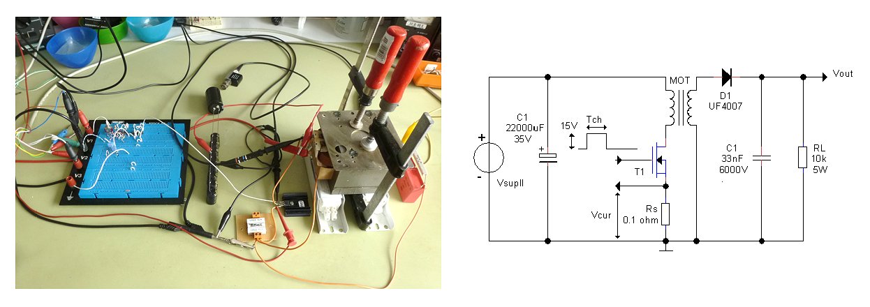
Figure 5.7 Improvised circuit used in the first pulse experiments.
Figure 5.8 shows some preliminary measurements using the setup described above. In this experiment an air gap of 1.25 mm was used. With this simple circuit it was possible to “charge” the transformer to 7 A (Fig. 5.8 left) with the power supply set at 30 V and a charging time of 20 ms. From the linear part of the charge curve the inductance was calculated to be 67 mH, which corresponds very well to the measured inductances listed in the table of Fig. 5.6: Lm + Ls = 50 mH + 12 mH = 62 mH. The leveling off of the increase in current is caused by the series resistances in the circuit. What is clear is the total absence saturation of the core, which would cause an exponential increase in current.
Attempts to further increase the current by increasing the length of the charging pulse resulted in frying of the MOSFET.
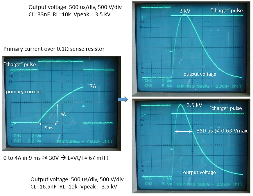
Figure 5.8 First pulse measurements using the MOT.
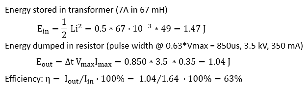
Even a current of “only” 7A was able to generate an high voltage pulse of 3 kV into a 10 kohm load, corresponding to a peak current of 300 mA and a peak power of 900 W. With two 33 nF capacitors at the output in series the output voltage further increased to 3.5 kV at a peak power of 1.225 kW, and a comfortable pulse width of 850 us at 63% of the maximum output voltage. If we evaluate the amount of energy stored in the transformer, and the energy dumped into the load (below), we find that what we could call the “conversion efficiency” amounts to approximately 63%. In this calculation only the losses in the core are taken into account, the resistive losses (at the primary side) are not included.
Concluding
Based on the calculations, simulations and first experiments it seems that the idea of a 5 kV / 1 A uTracer7 using a commonly available modified microwave oven transformer would not be an absolutely crazy idea. Although the transformers are designed for approximately 2.5 kV output voltage, I have no doubt that they can also perfectly handle 5 kV. In the end, due to the inevitable losses in the transformer, the target of 1 A in the end may appear to be a bit over ambitious, however, 0.5 A should certainly be possible. Unfortunately, the high “charging” current required, in combination with the resistance of the primary winding, will probably require some form of DC-DC conversion with the energy stored in a large reservoir capacitor. One of the original motivations of using an inductive energy storage element was safety; a magnetic field in an inductor cannot sustain itself due to resistive losses. However, the combination of a large low voltage capacitor with the up-transformer will again pose a safety issue. It will be paramount to add an interlock mechanism that will immediately discharge the capacitor after the circuit has been turned off.
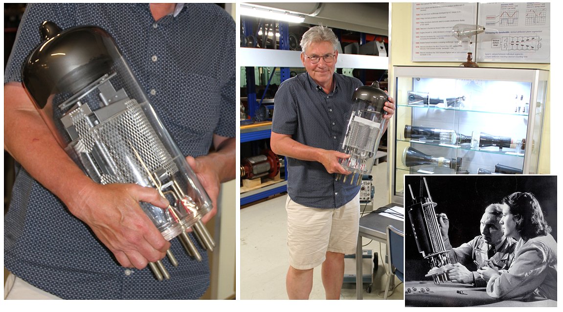
The Technical University of Delft in the Netherlands was founded in 1842. In the 180 years of its existence, it has obviously collected many historical artifacts. The objects related to electrical engineering are on display in the huge “Studieverzameling” (faculty collection) of the faculty of Electrical Engineering, Mathematics and Computer Science and is maintained by a large group of enthusiastic volunteers. Historically, the faculty had close ties with Philips, and the collection therefore contains many objects originating from Philips, like this huge model of an EL80 that was used to train Philips employees (insert). The collection is open to visitors on Mondays and Fridays for free. Worthwhile to have a look when you are in the neighborhood!
Link 1,
Link 2,
YouTube,
By far the most common and sensible way to continue would be to first perform circuit simulations before starting experiments. But I am so impatient to see if there is any sense in this crazy Microwave Oven Transformer (MOT) idea that I could not restrain myself and immediately started with a bench test setup.
Figure 6.1 shows the MOT interface circuit that was used in the first experiments. The parts of the circuit in the colored areas are the over-voltage protection circuit that has not been implemented yet. In Section 4 it was explained that the use of an inductive energy storage element like the MOT, results in a power source that has a current source character. After charging the inductor (or transformer), the output is a current pulse rather than a voltage pulse, and the voltage over the device under test is just the result of the current and the resistance (or impedance) of the load. This implies that if the resistance of the load is very high, the resulting voltage can become very high, with the risk of damaging components in the output section including the MOT. So, whereas in a voltage source some form of over-current protection is needed, for a current source an over-voltage protection is required. More about the over-voltage protection later.
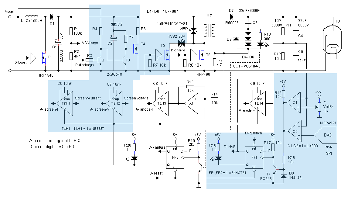
Figure 6.1 First sketch of the MOT interface circuit. The colored areas are the over-voltage protection circuit that has not been implemented yet.
Looking at the circuit in Fig. 6.1 we find the familiar boost converter circuit also used in the uTracer3&6 around transistor T1. The boost converter charges the enormous reservoir capacitor C1 which is rated at 22,000 uF / 63 V! Also in this case the boost converter is controlled by a PIC16F884 microcontroller. When charged, C1 is connected to the primary side of the MOT by transistor T6, which is an IRFP460 I happened to have lying around. The IRFP460 is rated at 500 V, a maximum pulsed drain current of 80 A and an Ron of 0.27 ohm. With a target maximum output peak voltage of 5000 V and a transformer ratio of 10, a bit higher breakdown voltage would be better, but it will have to do for now. An SIHA105N60EF-GE3 or SIHB105N60EF-GE3 are attractive and affordable 600 V alternatives with an Ron < 0.1 ohm. Not drawn in the schematic, but present in the test circuit is a 0.1 ohm current sense resistor in the source of T6. Commutation diode TVS1 absorbs the energy stored in the stray inductance of the transformer when T6 opens. In the initial experiments I used a 1.5KE440CA Transient Voltage Suppressor, which has a breakdown voltage of 460 V and a clamping voltage 600 V. We will see later that in practice the TVS clamped the output voltage at around 500 V.
Moving to the secondary side of the MOT, we basically find the circuit proposed in Fig. 5.7. Although I don’t think it is needed, I used a high speed R5000F-B diode specified at 5000 V breakdown. Recall that at the maximum output voltage, the current through C3 is exactly zero. To detect that moment, two antiparallel diodes have been connected in series with C3, whereby D3 is one of the diodes, and the series combination of D4, D5 and D6 the other one. When C3 is in the charging phase, the voltage drop across D4-D6 will be approximately 2 V, enough to turn on the LED in opto-coupler OC1. When the current through C3 changes polarity, the LED will turn off, signaling the peak in output voltage. For OC1 I selected an VO618A-3 because the required input current for the LED to switch on the phototransistor is only 1mA. Besides this is quite fast and very cheap! Resistor R9 senses the secondary current. By the way, note that C3 is grounded through R9 so that all the current through the load, apart from a very small and known current through the voltage divider at the output, is passed through R9. The output voltage is measured using a 1000:1 resistive voltage divider consisting of R11 and R12, which is frequency compensated by C4 and C5.
The primary reason to use an optocoupler in the pulse detection circuit was to effectively suppress any EMI noise that might arise from the switching of high currents. Apart from that, it of course provides a perfect isolation with the low voltage part of the circuit. When the LED in the opto-coupler switches off, flipflop FF2 is set, which causes the track & hold amplifiers T&H3 and T&H4 to capture the instantaneous output current and voltage. For the track & hold amplifiers I used an NE5537, which is an obsolete pin and function equivalent of the well-known LF398. By the way, the availability of stand-alone sample & hold circuits appears to be rather limited. Remarkable! Finally, no surprise, everything in the circuit is controlled by a microcontroller. For the first experiments, I used a very basic Arduino Uno.
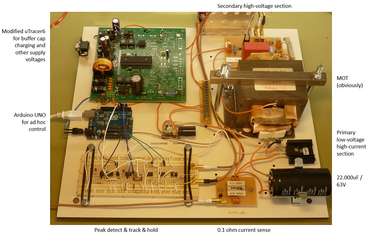
Figure 6.2 uTracer7 test bench.
Figure 6.2 shows the test bench for the “MOT uTracer7”. It is difficult to miss the MOT. By loosening the bolts, the two halves of the MOT can be separated so that it is possible to experiment with different air gap widths. Above the MOT is a perfboard with the high-voltage section. Top left a modified uTracer6 is used to charge the reservoir capacitor and to provide the +5, +15 and -15 supply voltages. Moving down we find the Arduino Uno board, and a breadboard with auxiliary components from Fig. 6.1. Finally, on the lower right we find the low-voltage, high-current part of the circuit.
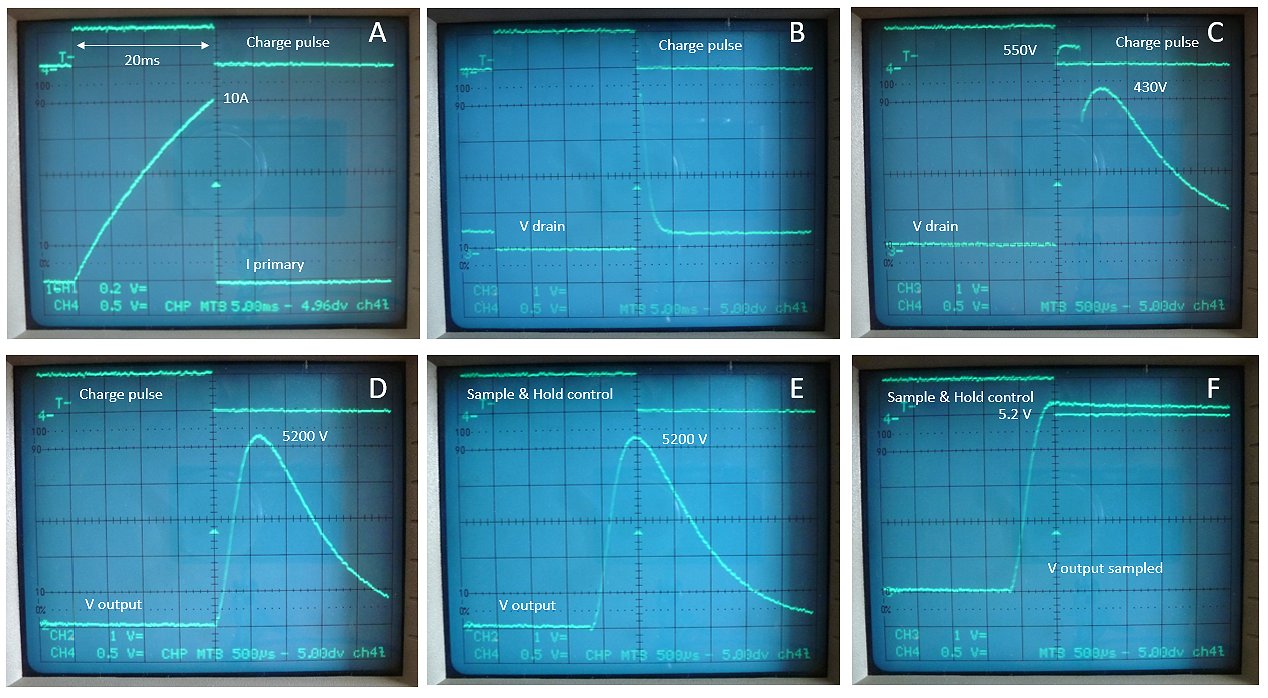
Figure 6.3 Typical voltages and currents at strategic points in the circuit for an input voltage (C1) of 50 V and a load resistor of 10 k.
Figure 6.3 shows various voltages and currents in the circuit. In this case the reservoir capacitor was charged to 50 V, and a 10 kohm resistor was used as load. The transformer was “charged” with a charge pulse of 20 ms. The top trace in Fig. 6.3A shows the charge pulse. The trailing edge of the charge pulse is used to trigger the memory scope as indicted by the small triangle in the center of the screen. The lower trace shows the current through the primary winding of the MOT. The current is measured by measuring the voltage drop over the sense resistor in the source of T6. With 2 A/div we see the current increase to 10A. The fact that the current doesn’t increase perfectly linearly is due to series resistances and discharging of C1.
Fig. 6.3B shows on the same time scale the drain voltage of T6. Compared to the “charging” time scale, the events that follow after T6 is opened only take a very short time. So in Fig. 6.3C the same signal is shown, but now at 500 us/div instead of 5 ms/div. We see that the drain voltage of T6 first jumps to 550 V. This is the stray inductance of the transformer “discharging,” or as they say commutating through the TVS. Since 50 V of this 550 V is due to the power supply voltage, we can conclude that the TVS is clamping the primary winding to 500 V. From the height and width of this pulse the stray inductance can be estimated. Since for an inductor I = (V*t)/L it follows that L = (V*t)/I = (500 V * 300 us)/10 A = 15 mH, which is close to what was measured in Fig. 5.6. After the stray inductance is discharged, the drain voltage drops to follow the voltage at the secondary side, be it not at the 520 V I would have expected, but at 430 V. This probably tells us that the transformation ratio is higher than expected (5200 V / 430 V = 12.1, rather than 10).
In Fig. 6.3D we move towards the output, measured through the 1:1000 voltage divider. So the vertical scale in this figure is 1000 V/div. The peak voltage is 5200 V resulting in a current of 0.52 A over the 10k load resulting in a peak output power of 0.27 kW. Figure 6.3E shows the same signal, but now the scope is triggered by the output of FF2 which controls the track-and-holds. Note that FF2 is triggered exactly at the peak of the output voltage. Figure 6.3F finally shows the output voltage of the track-and-hold. We see a small drop in voltage, but I have to see if this is real and if it is significant in relation to the conversion time of the ADCs.
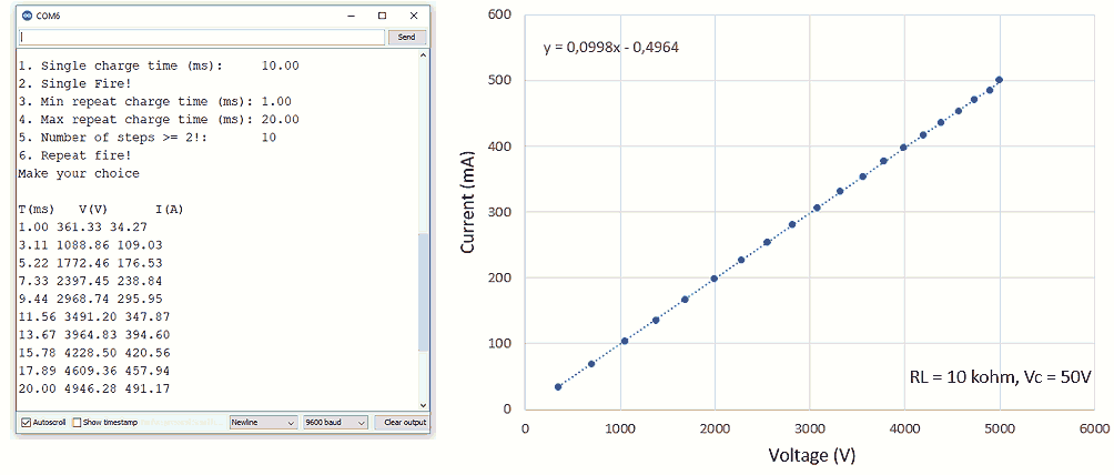
Figure 6.4 An example of an automatic sequence measured by a simple Arduin sketch.
For the time being, the circuit is controlled by a simple Arduino sketch, which controls various logic signals and converts and records the analog voltages. The sketch produces a simple menu that either generates a single pulse with a specified duration, or a series of pulses, linearly varying in duration between a minimum and maximum value (Fig. 6.4). The measured voltages and currents can be directly copied from the serial monitor into Excel. To my delight this produces perfectly linear measurements. Notice how the voltage and current increments slowly decrease as the charge pulse length becomes longer. This is of course due to the series resistances and discharging of C1. As discussed before, this is no problem, since the current – voltage pairs are sampled at the same time and each represent a true and valid point on the curve.
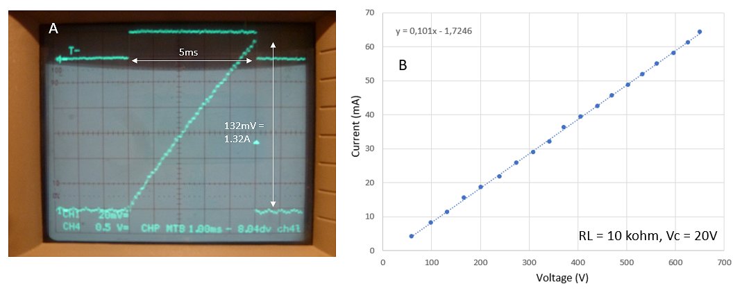
Figure 6.5 Behavior at “low” currents.
Figure 6.5 shows the working of the circuit in the low current regime. In this case the input voltage was reduced to 20 V, while the charge pulse width was varied between 0.3 and 5 ms. Again, here a perfect linear behavior that exceeds my expectations! For these “small” charging currents, series resistances can be neglected. This makes it possible to calculate the inductance seen at the input of the MOT. Using L = (V*t)/I, we find L = (20 V * 5 ms)/1.32 A = 75 mH. Since this is the sum of the magnetization inductance and the stray inductance (15 mH, see above), the magnetization inductance is 60 mH, which agrees nicely with the values listed in Fig. 5.6.
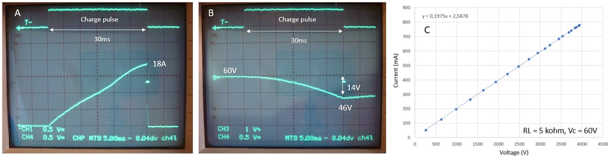
Figure 6.6 Pushing the limits.
In Fig. 6.6 the limits of the present configuration are explored. In this case a load of 5k was used and the input voltage was increased to 60 V, just below the maximum working voltage of C1. For charge pulses approaching 30 ms the output current, and thus the output voltage, saturated to approximately 800 mA at a voltage of 4000 V, a very respectable 3.2 kW peak power. Looking at the primary current we see that around 12 A the transformer starts to saturate. However, the current does not explode due to series resistances and the discharging of C1. After the the 30 ms pulse the voltage of C1 has dropped 14 V, corresponding to an energy loss of 0.5*C*(V1^2-V2^2) = 0.5 * 0.022 F *((60 V)^2 – (46 V)^2) = 16 J. Which, to give you an idea, is the energy needed to lift 16 apples up 1 m (assuming the apples have a mass of 101.97 g).
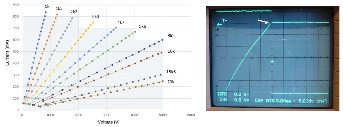
Figure 6.7 The “operating space” of the test circuit in its present configuration (left), and onset of saturation as indicated by the exponential increase in primary current (right).
In Fig. 6.7 the test circuit was connected to a series of different load resistors to get an idea of the “operating space” of the test circuit in its present configuration. For the lower resistance values (< 8k2), the maximum charge pulse length was reduced to just the onset of saturation, as indicated by the white arrow in the right picture. For the higher resistance values, the maximum charge pulse length was adjusted so that the maximum output voltage did not exceed 5000 V.
The colored area in the graph in Fig. 6.7 indicates the possible current/voltage combinations the present circuit can generate. I am pretty sure higher output voltages are possible, but I do not want to take the risk of damaging the primary switching transistor T6 or my modified MOT, which is already driven way beyond what it was designed for (2500 V). My initial goal of 5000 V @ 1A has not been achieved (yet), but we are getting close, and we still have one more trick in our sleeve: increasing the airgap in the MOT! Increasing the airgap will increase the current at which the core saturates, but lower the inductance. Assuming that for small changes in the airgap both will change more or less linearly, I expect that, since the energy stored is proportional to the inductance but proportional to the square of the current, it should be possible to push the performance a bit further. But before I try that, I want to order a transistor that can handle the higher currents and voltage!
Pushing the MOT to its limits
There is some time between the measurements shown above and this section because I wanted to order components to explore the limits of the MOT pulsed power supply. It appeared that if I tried to go to higher charging currents it would destroy the 1.5KE440CA, the Transient Voltage Suppressor diode TVS1, which absorbs the energy stored in the spreading inductance of the MOT. In retrospect that is no wonder; the momentary dissipation in the diode amounts to P = V * I = 550 V * 20 A = 11000 W (!!), be it only for approximately 0.5 ms (Fig. 6.3C). This obviously is too much for a TVS specified at pulsed dissipation of 1500 W and current of 3.1 A. It is actually quite a miracle that the diode survived up to this point! To be absolutely on the safe side, I replaced the 1.5KE440CA with eighteen 1.5KE33CA diodes in series. These diodes can take a peak current of 33 A while the peak dissipation is increased to 18 * 1500 W = 27000 W. At the same time I replaced the IRFP460 (T6) with a SQW44N65EF-GE3. This monster can handle 47 A @ 700 V combined with an on-resistance of 63 mOhm.
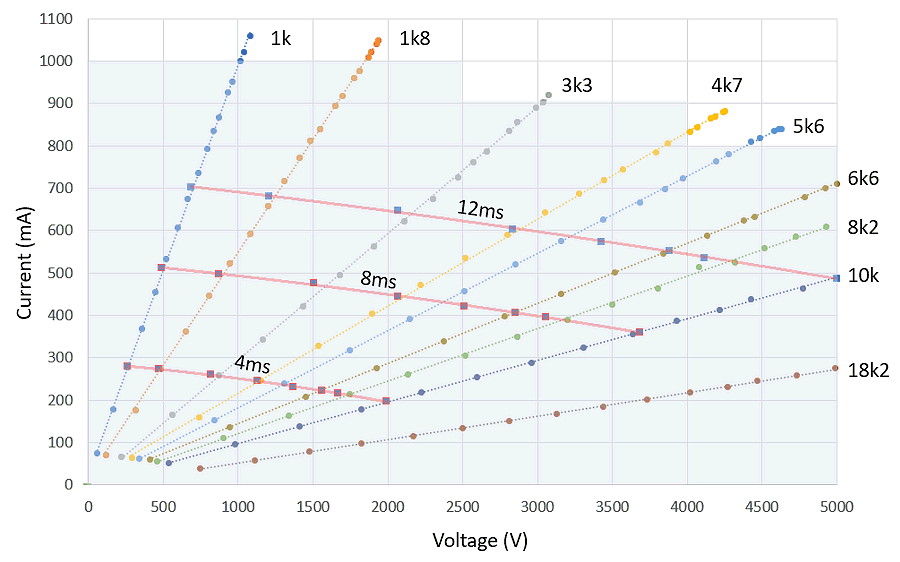
Figure 6.8 The MOT power supply pushed to the limits. The colored area indicates the maximum operating area of the pulsed MOT power supply.
The colored area in Fig. 6.8 indicates what I think is approximately the maximum operating area of the pulsed MOT power supply. The measurements are performed with C1 charged to 60 V, just bellow the maximum voltage at which it is specified. The airgap was increased to 1.84 mm. Again, for different resistive loads, the charging time was increased till the MOT saturates, indicated by a sharp increase in primary current. I am pretty sure the power supply is capable of much higher voltages, but I limited the charging time so that the maximum output voltage didn’t exceed 5000 V because I didn’t want to damage the MOT, which is already driven well beyond the 2500 V it is designed for. The solid lines in Fig. 6.8 were generated by varying the load resistor while the charge pulse width was kept constant. The fact that these lines are more or less horizontal show that the pulsed MOT power supply primarily has a current source behavior.
uTracer7 proposition
So, in summary, what do I have in mind for a MOT based uTracer7:
A sweep from 1 ms to 20 ms at 50 V input voltage with the uTracer7 test bench.
Shown on the oscilloscope is the voltage across the 10 k load resistor with the scale set at 1000 V/div.
So the maximum output voltage in this case is 5000 V @ 0.5 A.
The "ticking sound" is the core of the microwave transformer that is squeezed under the magnetic field.
Note that the sound is amplified by the freestanding board it is mounted on.
High level system overview
In this section a write-up of some uTracer7 ideas from a system level perspective. Again, like all writings in my blogs, they primarily serve for my own documentation, and everything may still change as the project evolves.

Figure 7.1 A first high level system overview of the uTracer7.
Figure 7.1 shows a simplified high-level block diagram of the uTracer7 as I have it in my mind right now. At first sight the circuit looks very complex, but things are not as bad as they seem because many of the blocks only contain a few components.
Let’s start with the most complicated part of the circuit, the pulsed anode supply. The principle of that circuit was already in detail explained in the previous section, but a short recap here. The microwave oven transformer (MOT) is powered by C2, a 22,000 uF / 63 V electrolytic capacitor. This capacitor in turn is charged by boost converter (D), which is controlled by the microcontroller. Since the current to which the primary side of the MOT is charged is in first approximation proportional to the product of the charging voltage and charging time, depending on the desired output current (and voltage), the voltage of C2 can be adjusted for a realistic and comfortable charging time.
The discharge circuit (E) has two functions. In the first place the PIC can activate this circuit to discharge C2 when the voltage of C2 needs to be reduced between measurements. The second function of the circuit is to discharge C2 for safety as soon as the main supply voltage is switched off.
As already mentioned, TVS1 absorbs the energy stored in the stray inductance of the MOT. It is drawn here as a single TVS, but in reality it will consist of a number of TVS diodes in series to absorb the current and energy that is being released. The moment of the peak output voltage is detected by sensing the current reversal through C3. During the charging of C3, optocoupler OC1 is activated, while diode D4 conducts the current during the discharge phase of C3. At the peak output voltage, OC1 triggers the peak detection circuit (F). The peak detection signals the sample and hold circuits to capture the anode voltage and current, the screen current, and the grid current. The peak detection circuit also notifies the PIC that an output voltage peak has been detected.
In “normal voltage source type of circuits,” the circuit is protected against too high output currents and short circuit situations by some form of a current limiting circuit or provision. In the uTracer7 anode supply, which is basically a current source, we need to protect the circuit against “over-voltage” conditions, e.g. when only a small output current is drawn or when the output is left open. Several circuit concepts were considered, but in the end I opted for the simplest solution by limiting the output voltage by means of a string of TVS diodes. The TVS diodes are selected in such a way that the user can choose to limit the output voltage to e.g. 1000 V, 2000 V, 3000 V, 4000 V or 5000 V by means of a hardware jumper. When an over-voltage occurs, it energizes optocoupler OC2. This in turn will trigger the over-voltage detection circuit (G) which notifies the PIC to take appropriate action. The reason why optocouplers are used in both circuits is basically for noise immunity. Both the peak detection as well as the overvoltage detection circuit are reset by the PIC.
The control grid is driven by a special high voltage OpAmp circuit (I) designed to generate output voltages between -200 V and 200 V. The circuit is built from discrete components and is asymmetrical in the sense that for positive output voltages it can source significant output currents (limit t.b.d.), while for negative output voltages it only needs sink a very small current. The grid bias circuit is powered by -210 V and +210 V boost converters (J,K). Since the positive grid bias will only be operated in pulsed mode, it is powered from capacitor C4 while the grid current is measured through a small current sense resistor in series with C4, just as in the positive grid extension board for the uTracer6. The discrete OpAmp in turn is driven by a DAC followed by a pre-amp. Since the discrete OpAmp inevitably will have a higher offset voltage than its integrated counterparts, the pre-amp serves to limit the voltage gain needed by the discrete OpAmp to the minimum.
Finally, the screen supply (A,B,C) will be identical to the high voltage supplies used in the uTracer6. For more information on this circuit, the reader is referred to the uTracer6 weblog. The last remaining circuit block is the -15 V boost converter power supply (M), that provides the negative supply voltage for the circuit.
Synchronization with the mains frequency
Most, if not all the transmitter tubes for which the uTracer7 is targeted, have very “heavy” heater requirements. A relatively “standard” Eimac 3-500Z for example draws a respectable 14.5 Amps at 5 V. The EIMAC 4-1000A shown in Fig. B.1 even draws 21 Amps at 7.5 V, a staggering 151 Watt! Fortunately, in RF transmitters, the heater of these mostly directly heated tubes can be an AC supply, so that a simple – be it a big – mains transformer can be used. However, as explained, the uTracer works in pulsed mode. This implies that without special precautions, the moment at which the voltages and currents are measured will be arbitrary with respect to the phase of the mains frequency. For directly heated tubes, this translates into a ripple, or noise on the grid – heater voltage that will result in “noisy” tube characteristics.

Figure 7.2 Synchronizing the measurements with the mains frequency to allow for AC heater powering of directly heated tubes.
For the positive grid extension board of the uTracer6 an option was introduced to synchronize the measurement pulse of the uTracer6 with the phase of the main frequency. As can be seen in Fig. 15-4 on that page, the solution works surprisingly well! Obviously, I plan to use the same trick for the uTracer7!
However, there is a snag. In the uTracer6 it is simply possible to charge the anode and screen capacitors to the desired voltage, and then wait with the measurement pulse until a zero-crossing in the heater voltage is detected. The situation for the uTracer7 is a bit more complicated; the actual moment of the measurement pulse is the result of a chain of close-coupled events that starts with the charging of the MOT, and ends with the detection of the peak in the output voltage. Figure 7.2 shows these events. At Tx transistor T1 (see Fig. 7.1) is closed, causing the primary current in the MOT to increase. At a certain moment (Tp) when the target primary current is reached, T1 is opened, and the energy stored in the MOT is transferred to C3 and subsequently to the output. The maximum output voltage is detected by the current reversal though C3, and at that moment (Tsample) the currents and voltages are captured. To synchronize the sample moment with the zero-crossing of the mains voltage as indicated in the graph, the moment Tx - when the charging of the MOT starts - must be carefully planned.
It should be realized that the time between the opening of T1 (Tp) and the moment of sampling – indicated by tpeak in the graph - is the only timing that is not controlled by the PIC, but determined by the secondary inductance (Ls) of the MOT, the capacitance of C3 and the load connected to the output. Fortunately, Ls and C3 are the dominant factors in this equation. For example, for my MOT and C3 = 22 nF, tpeak roughly varies between 150 us and 225 us going through the load conditions used to draw up Fig. 6.8. So, lets for the moment assume a tpeak of 200 us, we will discuss the consequences of a small timing error later.
Assume that at a certain moment the boost converters have charged all storage capacitors to their set point values and that the PIC is ready to issue a measurement pulse, implying that the desired charge time Tch is known. The PIC now starts waiting for the next zero crossing (T0) in the heater voltage. Now Tx (closing of T1) can be calculated from the formula given in Fig. 7.2. In this equation tres is a predetermined number of half mains periods (so in Europe 25 ms, 50 ms,75 ms ….), in any case longer than the maximum charge time encountered under normal operation.
Let’s estimate the consequence of a small timing error. Assume a sinusoidal heater voltage v(t) = Vh•sin(2πft). The derivative of the voltage gives the slope of the voltage dv/dt = Vh•2πf•cos(2πft). So in the zero crossing t=0, and dv/dt = Vh•2πf, assume f = 50 Hz, a heater voltage of 5 V and a maximum timing error of 100 us, then the upper bound for the error in the grid voltage is 2π•50•5•10-4 = 150 mV. Although this is certainly not negligible, it is very small compared to the grid voltage swing typically used for these high power tubes.
Similarly in this scheme the exact moment that the grid (screen and positive control grid) voltages are applied can be determined. The grid voltages need to be set before the anode voltage is applied because they require some set-up time (tsu) to settle. However, without the anode voltage present, the grids will draw excessive current, so tsu should be as short as technically possible. Similarly, the grid voltages need to be removed as soon as the voltages and currents have been sampled (Tsample). To make sure that the grids under no circumstances get overloaded:
Overvoltage protection
Most people are familiar with power supplies that behave like a voltage source. A voltage source outputs a constant voltage that will cause a current to flow through a load. Voltage sources need an overcurrent protection to protect both the voltage source, as well as the load against too high currents in case the resistance of the load is too low. Also the anode and screen supplies in the uTracer3 and uTracer6 have overcurrent protection circuits.
The idea of the uTracer7 is to use an inductive storage element to create a pulsed power supply which in first instance will behave not as a voltage source, but primarily as a current source (see also Section 4 of this page). Current sources don’t need an overcurrent protection, but they need an overvoltage protection that protects the source as well as the load against too high voltages in case the impedance of the load is higher than expected.

Figure 7.5 The overvoltage protection test circuit of the uTracer7.
Figure 7.5 shows a test circuit of the overvoltage protection I have in mind for the uTracer7. The basic idea is that the output is clamped by a string of Transient Voltage Suppressor (TVS) diodes. TVS diodes are a kind of high-power Zener, or more precise avalanche diodes, designed to shunt transient voltage spikes and absorb relatively large amounts of power. The idea is to use a string of TVS so that the user can set the maximum operating voltage in steps of approximately 1000 V, and at the same time distribute the total power over several TVS diodes.
To detect an overvoltage occurrence, the string of TVS diodes is placed in series with three normal diodes (D6-D8). In case of an overvoltage, the TVS diodes conduct the excess current causing a voltage drop over D6-D8. This energizes the LED in the opto-coupler, which in turn causes FF1 to be set, signaling to the PIC that an overvoltage has occurred. Just like in the peak detection circuit, the implementation with an opto-coupler was selected to maximize noise immunity.
When an overvoltage situation occurs, the worst-case scenario is that the TVS have to absorb all the energy that was stored in the MOT. So an important design question is how to dimension the string of TVS diodes in such away that this can happen in a safe way. It is important to realize that it is perfectly possible to place TVS diodes in series. In that way the total amount of power will be distributed over the individual diodes by ratio of their breakdown voltages.
I decided to use TVS diodes from a series that has a 1.5 kW peak pulse handling capability. This type of TVS diodes is very common, and several manufacturers have them available. I opted for the devices from Littelfuse. From the datasheet we find that these diodes are available with clamp voltages ranging from 6.8 to 600 V! Apart from the clamp voltage, the datasheet also specifies the maximum peak pulse current, which decreases with increasing voltage. What the datasheet doesn’t specify directly is the total amount of energy per pulse the TVS can handle. However, the datasheet does give a graph which specifies the maximum allowed peak-pulse power for a given pulse duration width (Fig. 7.7 left). And of course, power x time = energy, so although the shape of this pulse is accurately specified in the datasheet and we have a different pulse shape, it gives us some guideline.

Figure 7.6 Simplified output circuit used to calculate the clamp pulse width T.
The first step is to calculate the clamp pulse width. In the following calculation I assume that on the secondary side we “see” the transformed magnetization inductance Ls = n^2*Lm, with n the ratio of number of turns. To keep the math transparent, I calculate the energy needed to charge Ls with a constant voltage, instead of discharging it with a constant voltage, which basically boils down to the same thing. Figure 7.6 shows a simplified schematic of the high voltage output stage. For simplicity we neglect the capacitor and assume that the magnetization inductance as seen from the secondary side is discharged by a constant voltage V determined by the clamp TVS. We first calculate the amount of energy released into the TVS during the discharge. Next we equate that to the energy stored in the magnetization inductance at the primary side.

Figure 7.7 (right) shows an actual measurement. In this example the peak primary current was 18 A. With n = 10 and Lm = 53 mH the formula above yields 8 ms. The measured pulse width is 6 ms, which is reasonable agreement with this simple calculation. The fact that the measured pulse width is shorter, can obviously be attributed to the inevitable losses.

Figure 7.7 Left, peak pulse power (PPP) versus pulse width take from the datasheet. Right, the upper trace shows the output voltage, in this case clamped at 1250 V. The lower trace shows the overvoltage protection signal at the output of FF1.
Using the formula above, the second column in the table in Fig. 7.8 gives the clamp pulse width T for the five clamp voltages listed in column one. As expected, T decreases with increasing “discharge” voltage. In Fig. 7.7 (left) a graph from the datasheet is reproduced which gives PPP as a function of T. From the calculated pulse widths, we can now look up in the graph the permissible Peak Pulse Power PPP, which is listed in column three of the table. Multiplying PPP with T gives the maximum energy that may be dumped into the TVS, per event (column four).

Figure 7.8 Permissible and actual energy per TVS (see text).
Let’s use Peter’s giant MOT as an example. This MOT has a magnetization inductance of 54 mH and saturates around 20 A primary current. So fully charged that transformer releases to the secondary side an energy of E = 0.5*L*I^2 = 10.8 J, which has to be absorbed by the TVS diodes. Assume now that the TVS “ladder” is constructed from 500 V diodes (column five), then we can calculate the energy absorbed per diode by dividing 10.8 by the number of diodes (column six). Comparing column five to column three we observe that in the case only two diodes are used for the 1000 V clamp, we are just “on the edge” of what the diodes can tolerate. For higher voltages the absorbed amount of energy is less that the maximum value. So, although in practice, due to losses the amount of energy released will be less that 10.8 J, it may be advisable to realize the first “step” in the TVS ladder with e.g. four 250 V TVS diodes.
A new record!
My friend Peter got so enthusiastic about the project that he placed an advertisement for discarded microwave ovens in the local newspaper and collected a whole bunch of them. I never thought about it, but I foolishly always assumed that the maximum power of microwave ovens was 900 W at most 1000 W, but Peter found a German made Joker 629B oven that was rated at 1250 W! The oven contained a transformer that seemed huge compared to “normal” MOTs.


Figure 7.3 Top, Label on the Joker 629B microwave oven. Left, Peter’s brother opening the monster MOT with angular grinder. Right, the “standard” 1000 W MOT compared to the 1250 W MOT.
Peter’s brother helped him opening the transformer with his angle grinder. A delicate job, because you want to remove as little metal as possible. The designers of MOT transformers add space and magnetic shunts between the primary and secondary windings to increase the spreading inductance and so make the transformer more resilient against over-load conditions. However, to increase the efficiency of the transformer, Peter argued that it is necessary to reduce as much as possible the spreading inductance because all the energy that is stored in it will be lost. He removed the magnetic shunts and as much as possible all the material between the windings and additionally he managed to shift the primary winding approximately 6 mm upwards close to the secondary winding.

Figure 7.4 The 1250 W MOT pushed to the limit practically reaching 5000 V @ 1A, or 5000 W.

Figure 7.5 The “super” MOT compared to a “standard” MOT.
The test setup used in the previous sections was perfect to demonstrate and test the “MOT uTracer” principle. Now the next step is to construct a prototype uTracer7 “test-rig” around this concept, and test it on real tubes. The design objectives for this test uTracer7 are:
Circuit Diagram
This section discusses the circuit diagram of the uTracer7 as I have it this moment. As mentioned, large parts of the circuit like the control grid supply and the heater synchronization are still missing, and also the parts of the circuit that are presented here might still change. Because the circuit is becoming rather large, I have split it up into three parts: the power supplies, the processor and communications, and the anode and screen supplies. The component numbering in the circuit diagrams is still a bit of a mess. This is on one hand due to the fact that the heart of the experimental setup is a modified uTracer6, and I wanted to make sure that the part numbers of the components on the PCB correspond to the part numbers in the circuit diagrams, and on the other hand because I decided to stick with the part numbering convention I used for that uTracer:

Figure 8.1 General power supplies.
Figure 8.1 shows the circuit diagram of the general power supplies. This part is an almost one-to-one copy of the same circuit parts of the uTracer6, with the one exception that the voltage of the negative grid bias circuit has been increased from -85 V to -220 V. In the upper half of the circuit we find the very standard +15 V and +5 V linear regulators. Like in the uTracer3 and 6, again an old 19.5 V laptop power supply adaptor is used as the main power supply for the circuit. The boost converters in the anode and screen sections can draw very heavy current spikes from the power supply. L1 and C15 smoothen out these peaks somewhat for the comfort of the laptop adaptor.


Figure 8.2 CPU and communication section (top) and CPU pin designation (bottom).
The next re-used circuit part comprises the micro-controller and the serial communications (Fig. 8.2). The basic circuit didn’t change much compared to the uTracer6. However, several pins got new functions. In the test-rig the circuit is distributed over three PCB’s (Fig. 8.4). To keep track of the connections between the boards, I introduced mnemonics to label the different wires. The “to PCB#” column lists to which of the three boards a certain pin is wired: 1. central “uTracer6” pcb, 2. high voltage board, 3. control grid board.

Figure 8.3 Anode and screen section.
The anode and screen section (Fig. 8.3) is more interesting. At the top of the circuit we find the screen supply. The screen supply is largely identical to the uTracer6 HV supplies. There are a few changes. Whereas the uTracer6 HV supplies are referenced to the positive supply voltage, the uTracer7 screen supply is referenced to ground. Since normally the minimum output voltage of a boost converter cannot be lower than the supply voltage, this would mean that the minimum screen voltage is 19.5 V. Although I think that in practice this is not a problem, it is not very neat. By inserting a 24 V zener diode (D86) in series with the D80, the minimum output voltage is lowered to 0 V. The power loss in the zener will increase the charge time of C80/C81 a bit. If this is a problem in practice, D86 can simply be removed.
Note that the working voltage of C80/C81 has been lowered to 450 V. The main reason is that the 500 V types are only supplied by one manufacturer and sometimes have a very long lead time. This limits the maximum screen voltage to 900 V, but I guess that won’t be a problem for the screen supply. D81 has also been replaced by a zener diode which serves two purposes. During charging of C80/C81 the diode is forward biased as a normal diode, while during the measurement pulse, when the potential at the node of C81 and D81 is negative with respect to ground, it is reverse biased and protects the circuit against large negative spikes when the current is higher than expected, e.g. during a short at the output.
For the time being I decided not to incorporate the programmable gain amplifiers (PGAs) that were used in the uTracer3 and 6. Those uTracers were really meant for a broad range of tubes, ranging from low to medium power. The uTracer7 is designed for high power tubes only. Current ranging is simply achieved by adapting the current sense resistor. In the configuration shown in Fig. 8.3 the current range is 0 – 250 mA with S1 open, and 0 – 1 A with S1 closed. Another new feature of the screen supply is sample & hold IC82 which captures the screen current the moment when the maximum anode voltage is detected and at the same time also the anode current and voltage are captured. The high voltage switch circuit itself around T85 is identical to the circuit used in the uTracer6.
Below the screen section we find the main part of the anode supply. The circuit around T60 is a boost converter that charges C60 to an adjustable voltage with a maximum of 60 V. Zener diode D61 was added to lower the minimum voltage to 10 V at the expense of a somewhat longer charge time for higher voltages.
For safety reasons it is important that C60 is completely discharged when the circuit is switched off. Any remaining charge in C60 can potentially trigger a high voltage pulse at the output of the MOT. The circuit around T61, T62 and T63 is designed to discharge C60 as soon as the circuit is turned off. When power is connected to the circuit, C61 is charged but T63 is not conducting because T62 is conducting because its base is connected to Vsup through R63 and R64. However, as soon as the circuit is disconnected from Vsup, T62 is switched off and C60 is discharged through T63 and R66. Also during normal operation, discharging of C60 can be forced by the microcontroller switching on T61. LED3 was added as a crude means to indicate the charge status of capacitor C60. while there is any charge left in C60, LED3 will be on. It is essential that LED3 is a high intensity type.
The remaining parts of the circuit were already discussed in detail in the previous sections, so there is no point in me repeating it again here. The schematic circuit overview in the previous section links everything together.
Section 5 gives detailed explanation of the basic working of the MOT pulse generator around MOT1, T64, D63 and C62.
The anode voltage peak detection circuit configured around D64-D67, IC64 and IC66a is discussed in Section 6.
Finally, the overvoltage protection circuit around D68-D76, IC65 and IC66b is discussed in the previous section.
Download the TinyCad design files
Construction
If there is one thing I learned from the first test setup presented in the previous sections, it is that I wanted to have the MOT separate and detachable from the rest of the electronics. The massive weight of the MOT makes it otherwise practically impossible to work on the circuit. The overview photo at the end of this chapter shows how the MOT is separated from the electronics and connected to it by appropriate wiring and banana plugs.
Figure 8.4 Frontside of the uTracer7 test-rig.
Figures 8.4 and 8.5 show the top and bottom of the test-rig. It consists of four panels. The left most panel contains the banana plug receptacles that interface with the MOT, and the high current circuitry. A second lesson learned from the first test setup was to avoid as much as possible “open loops” in the wires that conduct the high primary charging current of the MOT. The high currents – up to 20 A! – in combination with the sudden opening of the primary charging transistor (T64) give rise to very high dI/dt transients which will induce magnetic fields that interfere with the rest of the electronics, e.g. prematurely setting of the flip-flops. By minimizing the open loop area in the high current circuit, e.g. by using simple mains twin cord (tweelingsnoer), the magnetic field generated by the current going in one direction is cancelled by the same current going into the opposite direction.
For the high-voltage wiring I used special silicone isolated high-voltage hookup wire rated at 15 kV. I was lucky enough to find a discarded spool with a considerable length of this wire left on it at work. Unfortunately, wholesalers like Mouser and Farnell only tend to offer this type of wire per complete spool at quite a high price. However, searching for it on internet I also found that Alibaba offers it per meter. Search for “high voltage hookup wire” or “spark plug wire” to find a supplier near to you.
On the bottom of the left panel is a small PCB with charging transistor T64 and the TSV string D63 which absorbs the energy stored in the leakage or spreading inductance when the MOT commutates. The transistor is a massive SQW44N65EF which combines an on-resistance of 73 mohm and a continuous drain current of 47 A with a breakdown voltage of 700 V. For the pulsed operation in the uTracer, no heatsink for the transistor is necessary. In series with the source of this transistor a 40 mohm current sense resistor is included to monitor the charging current of the MOT. The gate of the transistor is driven by the gate driver on the main PCB.
Figure 8.5 Backside of the uTracer7 test-rig.
The second panel/PCB from the left contains the high-voltage part of the circuit including the over-voltage protection TSV string. The desired clamping voltage can be set by connecting a jumper wire to the proper screw terminal. I sometimes tend to forget how high 5000 V really is, and in hindsight I could have made the layout of the high voltage section more spaciously.
Below the high voltage section are from left to right, the opto-couplers IC64 & IC65, the flip-flops IC66, sample & holds IC61 & IC63 and OpAmp IC62. The two LEDS labelled HV and Peak, respectively indicate a detected over voltage situation and the output voltage maximum peak. At the bottom of the PCB is the discharge circuit for C60. High intensity LED3 is a simple and reliable indicator of the state of C60. SMB connectors V and I directly give access to the real time output voltage and current. The sample & hold trigger signal and the MOT charge pulse are available to serve as scope trigger signals at connectors H and P.
In the center of the test-rig is a modified uTracer6 board. It contains the screen section with the modifications discussed in the previous section, the negative power supplies with the -85 V supply modified for -220 V, the microcontroller and a heavily modified anode section which is now used to charge C60. The heater section of the uTracer6 is omitted. On the backside of the board there is a switch board with the wiring that connects the two perfboards with the main board via 20 wire flat-cables provided with IDC connectors.
The rightest panel is still empty end reserved for the control grid supply, a +220V booster converter and the heater synchronization circuit.
Download layouts:
Figure 8.6 The test-rig in action. The two multimeters on the right monitor the MOT charging and screen voltages.


Firmware and GUI
The objective was to “quick and dirty” adapt the software to come as soon as possible to a fully functional prototype to test and explore uTracer7 concept. The software comprises three elements: the GUI, the communication between the GUI and the hardware, and the firmware in the microcontroller itself.

Figure 8.7 Appearance of the GUI after quick and dirty adaption for the uTracer7.
In the uTracers 3 and 6 you simply specify the voltages to be applied to the tube and then the uTracer measures the corresponding currents. What makes the uTracer7 concept completely different, is that while the grid and screen voltages are exactly specified, for the anode basically the amount of energy supplied to the anode is specified, resulting in a voltage-current pair. Although obviously a higher amount of energy usually will result in higher voltages and currents, there is no clear 1:1 relation between the amount of energy stored in the MOT, and the resulting voltage and current supplied to the anode. Apart from the losses in the MOT and electronics, the voltage applied to the anode strongly depends on the impedance of the tube. So, in this first version of the GUI the user can specify both the charging time as well as the charge voltage, more specific, the voltage to which C60 is charged before T74 is closed (Fig. 8.7). All this makes operating the circuit a bit tricky. For the future it is very well possible to envisage a clever algorithm that, based on measured voltages and currents, regulates the amount of energy stored in the MOT.

Figure 8.8 uTracer7 command structure compared to uTracer3&6.
For the time being, the operation of the uTracer7 is very simple. After the voltage of C60 is set (10-60 V), a sweep is made with increasing MOT charging times. Figure 8.8 top shows the command line structure of the uTracers 3&6. After the actual command, the anode, screen, grid and heater voltages are specified. Remember that the values that are sent by the GUI have already been translated in binary values which can be directly compared with the data from the 10-bit ADC of the PIC. Since the uTracer7 does not have a heater supply, that data word was re-used to set voltage of C60. In turn, the first data word that first was used to specify the anode voltage, is now used to specify the MOT charging time with a resolution of intervals of 100 us. Implementing the command structure in this way required the minimal number of changes in the GUI and firmware.

Figure 8.9 uTracer7 voltage & current conversion relations
Figure 8.9 gives the equations detailing how the different measured voltages and currents in the uTracer7 test-rig relate to the ADC output value. The GUI uses these relations to send the settings to the uTracer7 hardware and interpret the measurement results.
In all the uTracers the boost converters are controlled by an interrupt service routine that is called every 100 us. The main program enables or disables a particular boost converter and specifies the required voltages, after which the interrupt routine compares the setpunt value to the actual output voltage of a particular boost converter and issues boost converter pulses if needed. Read more about the boost converter control here and here. This program structure has two consequences:
The implementation of the measurement sequence in the uTracer7 is a bit of a tricky interplay between the main program and the interrupt service routine. Since no accurate timing is possible in the main program, the charging of the MOT is performed by the interrupt service routine, whereby the length of the charge pulse is determined by a specified number of calls to the interrupt service routine, which explains why the charge time resolution is 100 us. Figure 8.10 explains the implementation of the measurement sequence in more detail, whereby the left part depicts the actions in the main program, and the right part the flow in the interrupt service routine.

Figure 8.10 Implementation of a measurement sequence in the uTracer7.
Staring with the main program (left top), the first thing to be done in preparation for the measurement of the next data point is the charging of the anode and screen reservoir capacitors C60 and the pair C80&C81. Temporary variable n is used to count down the number of calls to the interrupt service routines, that is the number of 100 us intervals, so n is set to Tch. After the peak detect and overvoltage detect flip-flops have been reset, flag “charge” is set. The setting of this flag signals the interrupt service routine to take over control and start the MOT charging pulse (dashed line marked “A”). After setting the charge flag, the main program basically waits until the interrupt service routine has reset it.
Consequently on the very next call to the interrupt service routine on a timer 0 overflow, the interrupt service routine finds the charge flag set and knows it now has to deal with the MOT charging first, before dealing with the servicing of the boost converters. The first thing is does is switch on T64 and start (or continue) the charging of the MOT. Next it checks if n=10, or in other words, if we are now 1 ms before the switching off of T64 to stop the charging of the MOT. If so, all boost converters are switched off. This is to eliminate any noise the boost converters might introduce during the actual measurement of the currents and voltages. During the next two milliseconds, all analog circuits in the circuit are supplied by the charge stored in the reservoir capacitors of the supply boost converters. At the same time the screen and grid outputs are switched on. This has to happen immediately prior to the anode pulse to reduce the dissipation in the grid and screen in the absence of the anode voltage. Finally, the interrupt service routine checks if n has been decremented to zero. If it is not zero, n is decremented, and charging of the MOT continues for another 100 us. In case n=0 the charging of the MOT is completed and T64 is switched off causing the commutation of the MOT. Finally, the “charge” flag is reset to signal the main program that charging of the MOT has been completed.
The main program now resumes control (dashed line marked B). The first thing it does is to disable all interrupts. This stops any further calls to the interrupt service routine, making the AD converters available to the main program. The main program now waits for 1 ms. During this time the energy stored in the MOT is released at the secondary side of the MOT, resulting – if everything goes according to plan – in the high voltage anode output pulse. If everything works out as expected, the peak detect flip flop is set during this 1 ms interval. If not, it is signaled as an error condition. Also, the over-voltage flip flop is checked, and its status is communicated to the GUI to take further action. If all is ok, the currents and voltages stored in the sample and hold circuits are being read out for communication to the GUI. Finally, interrupts are enabled again, So the calls to the interrupt service routine at 100 us are resumed.
The final thing to be discussed is the screen over-current detection. In the uTracers 3&6, a screen (and anode) over-current protection mechanism was implemented, which is based on comparing the voltage drop over the current sense resistor with a programmable voltage. Both the comparators as well as the programmable voltage source are peripherals on the PIC (read more here). When an over-current situation occurs, the comparators cause an interrupt that switches-off the anode and screen power supplies. Although this mechanism is very fast, implementing it here at this moment would make the program less transparent. For the time being, the overcurrent protection is not on interrupt base, but simply by polling the comparator output during the wait loops in the main program.
My (former) colleague Peter has been mentioned already several times in these pages. With his huge knowledge in electronics and electro-magnetism, he has been, and I am happy to say still is, a fantastic discussion partner for all kind of aspects related to the uTracer projects. Peter worked in the magnetic recording group and in several research groups for integrated circuit design of analog and mixed-signal IC’s at Philips Research, for more than 40 years. With his expertise he helped me by making an LTspice model for my modified MOT. The model takes the physical dimensions of the MOT - including the airgap - as input, and includes saturation. The development of his model consists of the following steps:
Simplify the MOT structure
In Section 5 of this page I already made an attempt to simplify the MOT structure by halving the core and “inflating” the left-over half (Fig. 5.1). Although this worked, Peter uses a much more elegant simplification. Figure A.1-A again shows the core of my MOT, but now with accurately measured dimensions. What Peter did was simply cut the core though the middle, and fold the two halves together (Fig. A.1-B) so that we obtain a simple structure with double the width (Fig. A.1-C). Both the core area Acore and the magnetic path length of the core lcore are given in the same picture.

Figure A.1 Simplifying the MOT structure.
After removal of the magnetic shunts and the filament winding, we are left with a gap between the primary and secondary windings (Fig. A.2). This gap provides a path for magnetic flux between the windings that “flows” (I will come back to the word flow later) around only one of the windings and not through both. This will give rise to stray inductance that has to be considered.

Figure A.2 Figure (A) shows the flux path around both windings when one of the windings is excited and the other winding is left open (I=0). An induction voltage is generated in the other winding. Figure (B) shows a situation where stray inductance plays a role. Figure (B) shows the flux path around the primary winding (A) when the primary winding is excited and the secondary winding is short-circuited (V=0). An induction current is generated in the secondary winding, which counteracts / cancels the flux that otherwise would “flow” around the secondary winding. Figure (C) gives the dimensions of the stray inductance gap after removal of the magnetic shunts and the microwave filament winding.
Identifying the magnetic circuit
 In the previous section of this webpage, I calculated the inductance of the transformer using the very common method of calculating the magnetic resistances, or better reluctances, and then pretending the magnetic circuit behaves as an electrical circuit with a magnetomotoric force (mmf) acting as “voltage” sourse, and the “current” representing the magnetic flux. The advantage of this method, as Peter explains, is that the actual flux path topology, material properties and physical dimensions are taken into account, but a drawback is that the reluctance representation suggests that there is some kind of dissipation in the circuit, which is not the case.
The problem already starts with the word “flux,” which suggests that there is something flowing in the magnetic circuit, which is also not the case. Magnetic flux is not something flowing, but rather a condition, or state of the medium. In a piece of magnetic material like iron or ferrite in its initial state, all magnetic dipole moments are in a random orientation. If the piece of magnetic material is subjected to an increasing magnetic field strength, the dipole moments rotate a bit towards the magnetic field, initially only slightly, but eventually all of them are fully aligned, a state we call saturation. So, at a constant magnetic field strength there is nothing moving of flowing The situation is actually best compared to a capacitor where energy is stored in the polarized dielectric. A much more physical model is the so called gyrator-capacitor model. There is an excellent Wikipedia page that explains this model in a much better way than I can do. I will just reproduce the introduction to that page here:
The gyrator–capacitor model - sometimes also the capacitor-permeance model - is a lumped-element model for magnetic circuits, that can be used in place of the more common resistance–reluctance model. The model makes permeance elements analogous to electrical capacitance (see magnetic capacitance section on Wikipedia) rather than electrical resistance (see magnetic reluctance on Wikipedia). Windings are represented as gyrators, interfacing between the electrical circuit and the magnetic model (see picture to the right).
The primary advantage of the gyrator–capacitor model compared to the magnetic reluctance model is that the model preserves the correct values of energy flow, storage and dissipation. The gyrator–capacitor model is an example of a group of analogies that preserve energy flow across energy domains by making power conjugate pairs of variables in the various domains analogous. It fills the same role as the impedance analogy for the mechanical domain.
Figure A.3-A (below) shows the gyrator-capacitor model of the MOT proposed by Peter closely following the topology of the transformer. The different flux paths are represented by magnetic capacitances. The coloring inside the core1 and core2 capacitances denotes that in contrast to the other three capacitances these two are filled with a medium: the iron core. A further small simplification of the model is given in Fig. A.3-B, where the two identical airgap capacitances have been combined into a single capacitance with half the value. Finally, two gyrators represent the windings and form the bridge between the electrical and the magnetic domains (Fig. A.3-C). In Fig. A.3-D, as a first refinement to the model, the series resistances of the windings have been added.
Translation into a lumped element model
It is perfectly possible to construct a gyrator in LTspice from two voltage controlled current sources, and to include the gyrator-capacitor model directly into an LTspice simulation, resulting in a hybrid electro-magnetic circuit model. However, this is just a very simple problem, and just for my convenience Peter showed me how the magnetic circuit can be translated back into a lumped element electrical model. The trick Peter taught me was “to push” one of the gyrators through the circuit, whereby a series capacitor encountered in the magnetic domain translates into a parallel inductor in the electrical domain, while, you might have guessed it, a parallel capacitor is translated into a series inductor. The process is shown in Figs. A.3 E-H. After going through all the magnetic components, only the gyrators are left, and they “annihilate” each other resulting in an ideal (electrical) transformer (Fig. A.3-I).

Figure A.3 The gyrator-capacitor model of the MOT, and translation into an equivalent electrical lumped element representation. The core inductances are drawn as non-linear inductances because we want to include magnetic saturation. In below section we will investigate how to do that.
Inductances and saturation
An inductance L stores energy in the form of magnetic flux Φ. We all know the equation:


Figure A.4 shows a very clever LTspice demonstration circuit that Peter made to demonstrate the saturation model for the inductor (download the circuit here). There are two tricks worth explaining here. The first trick is that in LTspice, instead of specifying the inductance of an inductor, it is alternatively possible to specify the total magnetic flux in the inductor (as a function of current through the inductor). Just in the field where you would normally enter the value of the inductor, enter “flux={Φtot(x)}”, where Φtot(x) is an expression that gives the total magnetic flux as a function of the current x (equation 13 above). The second trick is that Peter uses a current source that produces a current ramp specified by the piecewise linear statement PWL(0 0 10 10). This produces a current starting at 0 A at t=0, linearly increasing to 10 A at t=10 s; so at a constant ramp of 1 A/s. The beauty of this is that the resulting voltage across the inductor is exactly equal to the inductance!

Figure A.4 Test circuit to demonstrate the inductor saturation model (download the circuit here).
The inductor in this example is the primary inductor of the MOT without airgap. According to the model the zero current inductance is 890 mH, which decreases to approximately half that value at 0.5 A.
The complete model
Figure A.5 shows the complete LTspice model for the MOT including saturation. A practical point is the addition of resistors Ra … Rd. These resistors are added because LTspice has difficulty in determining the DC bias point when two ideal inductors are connected in parallel. The same holds for two capacitors in series, but in this case LTspice adds two very high value resistances in parallel to the capacitors. It can do so without adding additional circuit nodes. This is not possible for two parallel inductors. So, adding a very small resistor in series with inductors helps LTspice to converge.

Figure A.5 The complete MOT model in LTspice format (click here to download it).
The values of the air inductance values directly follow from equation 15 with μr = 1. For convenience, the core is split in two equal halves with, as explained in the previous section, the total flux in the inductor as a function of current specified instead of the resulting inductance.
The ideal transformer has been implemented with a current controlled current source (F1) and a voltage controlled voltage source (E1). The use of the voltage controlled voltage source is straightforward. You just tie the controlling inputs to the relevant circuit nodes, the voltage across the current source in this case, and specify the gain. The current source does not have controlling inputs. For this component LTspice requires you to specify a controlling voltage source (by the way, it has to be a voltage source and not e.g. a resistor), followed by a gain. So two parameters. The working of the ideal transformer is easy to understand if you think a resistor R connected to the secondary side. Now imagine that we apply a voltage Vp at the primary side. This will cause an “amplified” voltage at the secondary side Vs = Vp * Ns / Np resulting in a current Is = Vs / R = Vp * (Ns/Np)/R. This current in turn, will cause a primary current Ip = (Ns/Np) * Is = Vp * (Ns/Np)^2/R at the primary side, and there we have our ideal transformer, even working for DC voltages!
Finally, resistor R3 was added to add some damping (losses) to the transformer as a result of eddy current losses in the core, as well as in the copper windings. The value of 6 kohm is just a starting point, final fine tuning of the value will need to be done empirically by matching simulation results to measurements.
Bernard Tellegen

The gentleman to the left is Bernard Tellegen. Tellegen was born the 24th of June 1900. He graduated from Delft University of Technology in 1923 in electrical engineering. After graduating, he joined Philips Research in Eindhoven where he became the first man in the new radio group headed by the legendary and eccentric Balthasar van der Pol.
Around that time, there was new safety legislation that limited the maximum anode voltage of radios. In that time only triodes were used as amplifying elements, and the lower anode voltage obviously also limited the audio volume. Tetrodes where known and produced more output power, but the kink in their output characteristics caused unacceptable distortion. Tellegen had the clever idea of inserting a third grid in between the screen grid and the anode to suppress the secondary electrons causing the kink. It worked brilliantly, and the pentode was born! A patent was granted, which, together with the patent on LOCOS isolation, generated hundreds of millions of licensing income for Philips.
Tellegen’s main specialism was network theory. He is known for Tellegen’s theorem, as well as the gyrator he postulated in 1948.
Next to his work at Philips, Tellegen he was extraordinary professor of network theory at Delft University of Technology from 1946 to 1966, where he received in 1970 an honorary doctorate. Tellegen was the recipient of many international awards, most famously he was the first non-American to receive the IEEE Edison Medal in 1973.
Until his death, Tellegen visited the library of Philips every week after which he enjoyed a sober lunch (picture). He died at the age of 90 in 1990.
For more stories and information about the early years of tube development at Philips, visit my pages on the development of the EF50 or the E1T tubes, and my lecture ”How a radio tube changed the world”, given at the occasion of 100 years Philips Research.
A resistor, although it can yield a lot of information, is not really the most exciting test object for the uTracer7. So, I started searching through my stash of tubes to look for a more plausible test object. Readers of my pages will know that I am not really “a tube man.” I will make a confession; I have never even made a tube amplifier myself! I just love tubes because of what they are, beautiful objects of craftmanship, and I am fascinated by the challenge of characterizing tubes with modern electronics. Nevertheless, I gathered an enormous collection of tubes over the years, including some heavy-duty transmitter tubes. The largest is an EIMAC 4-1000A power tetrode that will output 5000 W in the 110 MHz FM band, and I consider myself to be a lucky man that my wife also recognizes the beauty of these tubes so much that she placed it in the window in the living room. Pretty as the tube is, it draws a staggering 21 A heater current at 7.5 V. I also have a few EIMAC 3-500Z tubes that appear to be very popular among ham radio enthusiasts, but with 14.2 A at 5 V it is also not a convenient test tube to have on the test bench for quick experiments.
Then I found a couple of 8187 tubes. Especially the 8187 is an interesting tube:

Figure B.1 Left, my homebrew socket box with 8187 inserted. Center, output characteristics of the 8187. Right, an EIMAC 4-1000A decorating our living room window.
Because of its pulsed operation, the tube is not popular among ham radio and audio enthusiasts. So how did I get hold of them? That story takes us back into the history of Philips Research. When I joined Philips Research in 1988, Philips was in the middle of an enormous project called the “Mega-project.” Mega, as it was called by employees, was an alliance between Siemens and Philips to make an ultimate effort to break the Japanese hegemony in memory chips. New buildings were erected both at Philips Research in Eindhoven as well as in the then largest chip manufacturing site in Europe, Nijmegen, and at the same time hundreds of people were hired. Siemens was to concentrate on DRAM chips, while Philips would develop SRAM memory.
In the Semiconductor Research cleanroom in building WAG in Eindhoven, the first prototype memory chips were developed using the first photolithography steppers “the Silicon Repeater (SiRe)” developed by Philips. I spend the first years of my carrier working in that fantastic environment, although not working on CMOS, but on high-speed bipolar chips which were at that time still the workhorses for RF, television, and audio applications.

Figure B.2 The high-voltage room of the high-energy planter in building WAM at Philips Research. The cabinet on top of the high-voltage tower contained the ion source. The ions were accelerated in the isolating tube indicated by the arrow. Photo’s taken early 1984.
One of the key technology steps that was deemed necessary for the next generation CMOS chips was high-energy ion implantation for the fabrication of deep n-wells and p-wells. Together with the Dutch National Institute for Subatomic Physics NIKHEV, that had the necessary expertise in particle acceleration, an enormous high energy implanter was built. The implanter could implant with an energy of up to 1 MeV and occupied two large rooms in building WAM. The ions were generated in the “high-voltage room,” which was basically a huge cage of Faraday, with shielded walls and rounded corners (Fig. B.2). In the center of the room was a “high voltage tower” with at the top a cabinet containing ion sources, mass separation magnet, PLC and a power generator that was driven by a rotating plastic shaft driven by a motor underneath the floor. The whole cabinet could be lifted to a voltage of up to 1 MV. The ions generated in the high voltage cabinet where accelerated in an isolated tube from the high positive voltage in the cabinet to ground potential at the wall where the left the cage of Faraday and entered the control room.
In the control room the ions travelled through a long tube to a “magnetic switch” where they could be directed to one of the two end stations containing the silicon target wafers (Fig. B.3). The final tubes leading to the end stations contained large horizontal and vertical deflections plates that scanned the ion beam over the wafer surface. Finally, you already feel the punch line coming, these defection plates were driven by 8187 tubes.

Figure B.3 The control room of the high-energy implanter. In the center of the two “legs” leading to the end-stations the ions enter the room to be subsequently directed to one of the two end-stations. The ion bundle is scanned by vertical and horizontal deflection plates connected to the scanning electrons at the points indicated by the arrows. Left picture 1996, right picture 1984.
The Mega project was not a commercial success. Siemens already very quickly realized that they would not survive on their own, and quickly forged an alliance with Toshiba. Philips, struggled for a few years on their own with their Megabit SRAM chips for which there basically was no market, until around 1993 when the losses amounted to nearly 1 million guilders a day, the then president Jan Timmer abruptly terminated the activity, saving Philips from bankruptcy. They high energy implanted survived for many years until after the transfer of all the semiconductor related research to IMEC in Leuven it was closed and subsequently scrapped in the first years of the new millennium. The tubes and sockets I have come from the enormous stock of spare parts in the cellars underneath the implanter.
Although by itself the Mega project was not a success, the knowledge on silicon photolithography steppers found its way to the young startup ASML, now the world leader in deep submicron lithography and by far the largest employer in the region. Much of the processing knowledge was transferred to TSMC of which Philips was one of the founders with an original share of 40%
| to top of page | back to uTracer homepage |
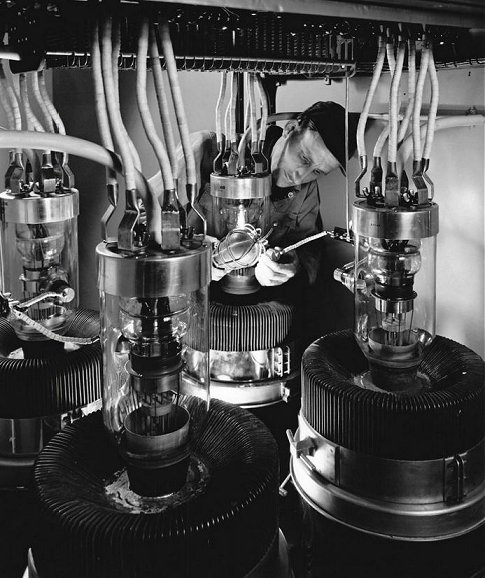